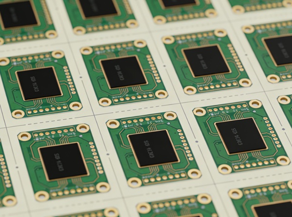
PCB panelization is widely used in electronics manufacturing to improve production efficiency. Instead of producing individual boards separately, multiple PCBs are grouped together into a larger panel during fabrication and assembly.
Panelization provides several advantages:
- Higher manufacturing efficiency
- improved assembly automation
- reduced production cost
- easier handling during fabrication
However, poor panel design can lead to problems such as board warpage, depanelization damage, and assembly misalignment.
Understanding PCB panelization design guidelines helps engineers ensure that boards are manufactured and assembled efficiently.
Indholdsfortegnelse
What Is PCB Panelization?
PCB panelization is the process of arranging multiple PCB designs into a larger panel for fabrication.
A typical PCB production panel may contain:
- several identical boards
- different board designs
- test coupons and tooling areas
After assembly, the boards are separated from the panel using depanelization methods.
The complete PCB fabrication workflow is explained in: PCB-fremstillingsproces forklaret
Why PCB Panelization Is Important
Panelization improves both manufacturing efficiency og assembly reliability.
Key benefits include:
Efficient PCB fabrication
Processing larger panels increases throughput and reduces setup time.
Improved assembly automation
Pick-and-place machines handle panels more easily than individual boards.
Reduced handling damage
Panels provide mechanical stability during assembly processes such as solder paste printing and reflow.
Lower manufacturing cost
Panelization maximizes material utilization and reduces waste.
The relationship between manufacturing efficiency and cost is discussed in: Sådan reducerer du PCB-omkostningerne uden at gå på kompromis med kvaliteten
Common PCB Panelization Methods
Different panelization methods are used depending on board geometry and production requirements.
V-Cut (V-Score) Panelization
V-cut panelization uses shallow V-shaped grooves along board edges.
Karakteristika:
- Boards remain connected during assembly
- separation occurs after assembly
- suitable for rectangular boards
Fordele:
- simple design
- lower fabrication cost
Begrænsninger:
- not suitable for irregular board shapes
Tab Routing Panelization
Tab routing uses small breakaway tabs to connect boards within the panel.
Funktioner:
- Routed edges define board outlines
- Small tabs hold boards in place
- mouse-bite perforations assist separation
Fordele:
- supports complex board shapes
- flexible panel layouts
Solid Rail Panelization
Some panels include additional rails along the edges.
Rails are used for:
- conveyor transport
- placement machine gripping
- fiducial placement
Assembly rails are removed after manufacturing.
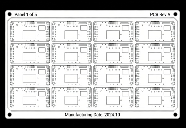
PCB Panel Size Guidelines
Panel size depends on both fabrication equipment and assembly machines.
Typical panel sizes:
| Panel Type | Typisk størrelse |
|---|---|
| Standard PCB panel | 18 × 24 inches |
| Smaller production panels | 12 × 18 inches |
Panel sizes should align with manufacturer capabilities.
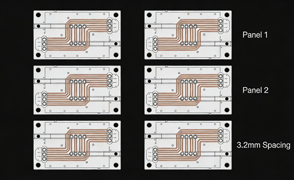
Board Spacing in Panel Design
Spacing between boards is required for routing tools or V-cuts.
Typical guidelines:
V-cut spacing: 0 mm (shared edge)
Tab routing spacing: 2–3 mm
Adequate spacing prevents mechanical damage during depanelization.
Tooling Holes and Fiducial Marks
Panelization must include reference features for assembly equipment.
Tooling holes
Used for mechanical alignment during assembly.
Typical guidelines:
- 3 mm diameter holes
- located near panel corners
Fiducial marks
Used by pick-and-place machines for optical alignment.
Types:
- global fiducials (panel level)
- local fiducials (component area)
Proper alignment improves placement accuracy.
How to Design a PCB Panel (Step-by-Step)
Ingeniører følger typisk en struktureret proces, når de laver panellayout.
- Trin 1 - Bestem produktionsmængden
Prototyper i små mængder kræver måske ikke kompleks panelisering.
- Trin 2 - Vælg paneliseringsmetode
Vælg V-cut eller tab routing baseret på pladens form.
- Trin 3 - Definer panelskinner
Tilføj skinner, hvis monteringsudstyret kræver ekstra støtte.
- Trin 4 - Placer referencer og værktøjshuller
Sørg for, at maskinerne kan justere panelet nøjagtigt.
- Trin 5 - Kør DFM-tjek
Producenterne kontrollerer, at panellayoutet er kompatibelt med produktionsudstyret.
DFM-gennemgangsprocessen er forklaret i: PCB DFM-tjekliste før afsendelse af Gerber-filer
Common PCB Panelization Mistakes
Several common design errors can affect manufacturing efficiency.
Panels without assembly rails
Some automated assembly systems require rails for conveyor transport.
Insufficient spacing between boards
Boards may crack during depanelization.
Missing fiducial marks
Placement machines may experience alignment errors.
Weak breakaway tabs
Panels may break prematurely during assembly handling.
Overvejelser vedrørende fremstilling
PCB manufacturers usually review panel layouts during CAM engineering analysis.
De evaluerer:
- panel dimensions
- board spacing
- depanelization methods
- rail design
- fiducial placement
At PCB manufacturers such as TOPFAST, panelization designs are often optimized during the engineering review stage to improve both fabrication efficiency and assembly reliability.
Konklusion
PCB panelization is an important step that connects PCB design with manufacturing and assembly processes.
By following panelization design guidelines—such as appropriate panel sizes, spacing rules, and breakaway methods—engineers can significantly improve production efficiency and reduce manufacturing risks.
Proper panel design also ensures compatibility with automated assembly systems and helps maintain consistent production quality.
OFTE STILLEDE SPØRGSMÅL
A: PCB-panelisering er processen med at kombinere flere printkort til et enkelt panel til fremstilling og samling.
A: V-cut bruger riller langs pladekanterne til adskillelse, mens tab routing forbinder plader ved hjælp af breakaway tabs med perforeringer.
A: Fiducialmærker hjælper automatiserede monteringsmaskiner med at justere panelet nøjagtigt under placering af komponenter.
A: For tab routing er afstanden typisk 2-3 mmmens V-skårne paneler kan dele kanter med minimal afstand.