Die Leiterplattenherstellung ist eine mehrstufiger, streng kontrollierter Prozess wo kleine Abweichungen zu Zuverlässigkeitsproblemen, Ertragsverlusten oder erhöhten Kosten führen können.
Während viele Ressourcen die Leiterplattenherstellung auf hohem Niveau beschreiben, ist das Verständnis wie jeder Fertigungsschritt mit dem nächsten zusammenhängt ist entscheidend für:
- Entwurf von herstellbaren Platten
- Kostenkontrolle
- Gewährleistung langfristiger Zuverlässigkeit
Dieser Artikel enthält eine Schritt-für-Schritt-Übersicht über den PCB-Herstellungsprozessmit Links zu ausführlichen Erläuterungen zu jeder kritischen Phase.
Die Perspektive spiegelt die realen Herstellungspraktiken professioneller Leiterplattenhersteller wider, wie z. B. TOPFASTwo Prozessstabilität und Ertragskontrolle zentrale Prioritäten sind.
Inhaltsübersicht
Überblick über die PCB-Herstellungsprozess
Ein typischer Arbeitsablauf bei der Herstellung von Leiterplatten umfasst:
- Herstellung der inneren Schicht
- Bohren (mechanisch oder Laser)
- Verkupfern
- Ätzen von Mustern
- Inspektion und Ertragskontrolle
Jeder Schritt baut auf dem vorhergehenden auf. Fehler, die zu Beginn des Prozesses gemacht werden, können später oft nicht mehr korrigiert werden.
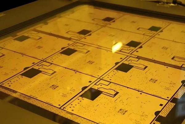
Herstellung der inneren Schicht
Die Herstellung der inneren Schicht ist die Grundlage der Herstellung von Mehrlagen-Leiterplatten.
In diesem Stadium:
- Die Kupferfolie ist so strukturiert, dass interne Schaltkreise entstehen
- Maßhaltigkeit ist entscheidend
- Defekte sind nach der Laminierung dauerhaft im Stapel eingeschlossen
Da die Innenschichten nach dem Laminieren nicht mehr repariert werden können, wenden die Hersteller strenge Prozesskontrollen und Prüfstandards an.
Eine ausführliche Erläuterung der Vorbereitung der Innenschicht, der Bildgebung und des Ätzens finden Sie unter:
Inner Layer Fabrication erklärt
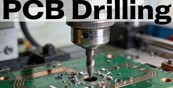
PCB-Bohrungen: Erstellen von Zwischenlagen-Verbindungen
Durch das Bohren entstehen die Löcher, die später zu Durchkontaktierungen und Durchsteckverbindungen werden.
Es werden hauptsächlich zwei Bohrverfahren angewandt:
- Mechanisches Bohren
- Laserbohren
Jede Methode bringt Kompromisse mit sich:
- Größe des Lochs
- Seitenverhältnis
- Kosten
- Verlässlichkeit
Unsachgemäßes Bohren wirkt sich direkt auf die Qualität der Beschichtung und die Zuverlässigkeit des Systems aus.
Lesen Sie, wann mechanisches Bohren oder Laserbohren angebracht ist:
Leiterplattenbohren vs. Laserbohren
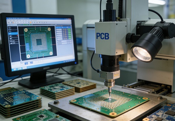
Verkupferungsprozess
Die Verkupferung verwandelt gebohrte Löcher in elektrisch leitende vertikale Verbindungen.
Der Beschichtungsprozess umfasst:
- Stromlose Kupferabscheidung
- Elektrolytische Kupferdickenbildung
Die Qualität der Beschichtung entscheidet:
- Über die Wandstärke
- Thermische Zyklusleistung
- Strombelastbarkeit
Inkonsistente Beschichtungen sind eine häufige Ursache für Ausfälle im Feld, selbst wenn die Leiterplatten die ersten elektrischen Tests bestehen.
Eine vollständige Aufschlüsselung der Beschichtungsstufen und Überlegungen zur Zuverlässigkeit finden Sie unter:
Verkupferungsprozess in der PCB-Herstellung erklärt
PCB-Ätzen und Schaltungsentwicklung
Beim Ätzen wird unerwünschtes Kupfer entfernt, um das endgültige Schaltungsmuster zu definieren.
Dieser Schritt muss ausgewogen sein:
- Dicke des Kupfers
- Genauigkeit der Linienbreite
- Kontrolle der Abstände
Überätzung oder Unterätzung führt zu:
- Offene oder kurze Hosen
- Änderung der Impedanz
- Geringerer Produktionsertrag
Die Ätzleistung wird zunehmend kritischer, da die Designs immer feinere Leiterbahnen und höhere Schichtzahlen aufweisen.
Einen detaillierten Einblick in die Ätzchemie und die Auswirkungen auf den Ertrag erhalten Sie in diesem Artikel:
PCB-Ätzprozess und Ertragskontrolle erklärt
Ausbeutekontrolle über den gesamten Herstellungsprozess
Die Ausbeute wird nicht in einem einzigen Schritt kontrolliert - es ist die Ergebnis der kumulativen Prozessstabilität.
Zu den wichtigsten Ertragsfaktoren gehören:
- Genauigkeit der inneren Schicht
- Qualität der Bohrer
- Gleichmäßigkeit der Beschichtung
- Konsistenz der Ätzung
Professionelle Leiterplattenhersteller überwachen kontinuierlich die Ertragsdaten, um:
- Identifizierung von Prozessabweichungen
- Optimieren Sie Entwurfsregeln
- Reduzierung von Ausschuss und Nacharbeit
Bei TOPFAST wird die Rückmeldung über die Ausbeute in die DFM-Prüfungen integriert, um den Kunden zu helfen, versteckte Fertigungsrisiken zu vermeiden, bevor die Produktion beginnt.
Einen auf das verarbeitende Gewerbe ausgerichteten Überblick über Renditetreiber finden Sie unter:
PCB-Ätzprozess und Ertragskontrolle erklärt
Wie sich Designentscheidungen auf den Herstellungsprozess auswirken
Vom Standpunkt der Fertigung aus betrachtet, haben viele PCB-Probleme ihren Ursprung in Design-Entscheidungen wie z. B.:
- Zu feine Leiterbahnbreiten
- Vias mit hohem Aspektverhältnis
- Unsymmetrische Kupferverteilung
- Übermäßig enge Toleranzen
Eine frühzeitige Zusammenarbeit zwischen Konstrukteuren und Herstellern hilft, die Konstruktionsabsicht mit der Prozessfähigkeit in Einklang zu bringen.
Dieser Ansatz reduziert:
- Wiederholungen
- Verzögerungen bei der Produktion
- Gesamtbetriebskosten
Die Perspektive des Herstellers: Prozessintegration bei TOPFAST
Als professioneller PCB-Hersteller betrachtet TOPFAST die PCB-Fertigung als eine integriertes Systemund nicht einzelne Schritte.
Zu den wichtigsten Grundsätzen gehören:
- Stabile Prozessfenster
- Frühzeitige Identifizierung von DFM-Risiken
- Ertragsabhängige Optimierung
- IPC-konforme Qualitätsstandards
Anstatt sich nur auf Mindestanforderungen zu konzentrieren, liegt der Schwerpunkt auf Wiederholbarkeit, Zuverlässigkeit und skalierbare Produktion.
Schlussfolgerung
Der Herstellungsprozess von Leiterplatten ist eine Abfolge von voneinander abhängigen Schritten, bei denen die Qualität schrittweise aufgebaut und nicht erst am Ende geprüft wird.
Wenn Ingenieure und Einkäufer verstehen, wie die Herstellung von Innenschichten, das Bohren, Verkupfern und Ätzen zusammenarbeiten, können sie das:
- Bessere Designentscheidungen treffen
- Reduzieren Sie das Herstellungsrisiko
- Kostenkontrolle ohne Qualitätseinbußen
Dieser Überblick dient als Tor zu tiefer gehenden technischen Erklärungen für jede kritische Phase und spiegelt die realen Praktiken wider, die von erfahrenen PCB-Herstellern wie TOPFAST.