Was ist eine Hochgeschwindigkeits-Leiterplatte? Design-Leitfaden
Inhaltsübersicht
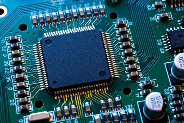
Was ist ein Hochgeschwindigkeits-Leiterplatte?
Einfach ausgedrückt: Wenn die Anstiegs-/Abfallzeit eines digitalen Signals so kurz ist, dass die physikalischen Eigenschaften der Leiterbahnen auf der Leiterplatte – wie Impedanz, Verzögerung und parasitäre Effekte – einen erheblichen Einfluss auf die Signalqualität ausüben, fällt die Leiterplatte in die Kategorie der Hochgeschwindigkeits-Leiterplatten.
Die Bedeutung von Hochgeschwindigkeits-Leiterplatten
Im heutigen Zeitalter der Hochgeschwindigkeitsdigitaltechnik, von Smartphones bis hin zu Servern in Rechenzentren, hängen die Leistungsengpässe von Geräten zunehmend von der Fähigkeit ihrer internen Leiterplatten ab, Hochgeschwindigkeitssignale zu übertragen und zu verarbeiten.Es ist wichtig zu beachten, dass „Hochgeschwindigkeit“ nicht allein durch einen bestimmten Frequenzwert definiert wird, sondern in engem Zusammenhang mit der Änderungsrate der Signalflanken und der Länge des Übertragungswegs steht. Daher hat sich das Kernziel des Hochgeschwindigkeits-Leiterplattendesigns von der traditionellen Fokussierung auf die Gewährleistung der „elektrischen Konnektivität“ zu der kritischeren Aufgabe der Aufrechterhaltung der „Signalintegrität“ verlagert.
Was ist Hochgeschwindigkeits-Leiterplatten-Design?
Das Design von Hochgeschwindigkeits-Leiterplatten ist ein systematischer technischer Ansatz, der sich auf die Analyse und Kontrolle verschiedener Probleme konzentriert, die bei der Übertragung von Signalen auftreten können.In Niederfrequenzschaltungen können Leiter als ideale „kurze Leitungen” approximiert werden, in denen Signale nahezu augenblicklich übertragen werden. In Hochgeschwindigkeitsszenarien sind Leiterbahnen auf Leiterplatten jedoch nicht mehr nur einfache elektrische Verbindungen, sondern müssen als Übertragungsleitungen modelliert und analysiert werden. Wenn die charakteristische Impedanz von Übertragungsleitungen nicht übereinstimmt, kann dies zu Signalreflexionen, Klingeln oder Überschwingungsphänomenen führen, was Datenfehler oder sogar Systemausfälle zur Folge haben kann.
Daher geht es beim Design von Hochgeschwindigkeits-Leiterplatten um mehr als nur darum, „die richtigen Punkte zu verbinden“. Es erfordert eine umfassende Berücksichtigung von Faktoren wie elektromagnetischen Feldeffekten, Impedanzkontrolle, Übersprechen, Timing und Stromintegrität während der Front-End-Designphase. Dadurch wird die Signalqualität während des gesamten Übertragungsprozesses vom Sender zum Empfänger sichergestellt.
10 praktische Tipps für das Design von Hochgeschwindigkeits-Leiterplatten
Frühzeitige Zusammenarbeit mit Herstellern
Wenden Sie sich an Ihren Hersteller von Hochgeschwindigkeits-Leiterplatten (z. B. TOPFAST) während der ersten Phase der Layout-Entwicklung, um Vorschläge zum Stack-up und zu den Möglichkeiten der Impedanzsteuerung zu besprechen und sicherzustellen, dass das Design mit den Prozessspezifikationen übereinstimmt.
Definieren Sie eine klare Stapelstrategie
Weisen Sie bestimmte Ebenen im Lagenaufbau für Strom-, Masse- und kritische Signalschichten zu, um eine stabile Impedanz und eine effektive Geräuschisolierung zu gewährleisten.
Simulationsgestütztes Design
Führen Sie sowohl vor als auch nach dem Layout Signalintegritäts- (SI) und Stromintegritäts- (PI) Simulationen durch, um potenzielle Probleme proaktiv zu identifizieren und zu mindern.
Strikte Einhaltung der Impedanzberechnungen
Berechnen Sie die für die Zielimpedanz erforderliche Leiterbahnbreite und den Abstand präzise und erzielen Sie diese Werte, indem Sie sich streng an die vom Hersteller angegebenen Materialparameter (z. B. Dielektrizitätskonstante, Dk) halten.
Sicherstellen, dass Referenzebenen nicht unterbrochen werden
Hochgeschwindigkeits-Signalleitungen für kritische Signale müssen über eine solide Referenzebene (Masse oder Stromversorgung) verfügen. Vermeiden Sie Kreuzungen in der Referenzebene, um einen klaren Rückweg zu gewährleisten.
Differentialpaar-Routing optimieren
Halten Sie eine konsistente Breite, einen konsistenten Abstand und eine konsistente Parallelität für Differentialpaare ein und kontrollieren Sie streng die Längenanpassung innerhalb der Paare, um die Störfestigkeit und Signalqualität sicherzustellen.
Entkopplungskondensatoren in der Nähe der Pins platzieren
Positionieren Sie Entkopplungskondensatoren so nah wie möglich an den Stromanschlüssen der ICs, um die Schleifeninduktivität zu minimieren und eine effektive Filterung von Hochfrequenzrauschen zu gewährleisten.
Vermeiden Sie spitze Winkel
Verwenden Sie für alle Signalverlaufsbiegungen 135-Grad-Winkel oder Bogenverläufe, um Impedanzdiskontinuitäten und Signalreflexionen zu minimieren.
Signalrückwege verwalten
Berücksichtigen und kontrollieren Sie stets den Rückstrompfad von Hochgeschwindigkeitssignalen und stellen Sie sicher, dass er niederohmig bleibt, was für die Aufrechterhaltung der Signalintegrität von entscheidender Bedeutung ist.
Priorisieren Sie Ground Vias in der Nähe von Schichtübergängen
Platzieren Sie Ground-Vias neben Signal-Vias, wenn Hochgeschwindigkeitssignale die Schicht wechseln, um den kürzesten, durchgehenden Rückweg mit niedriger Impedanz zu gewährleisten.
Warum benötigen Hochgeschwindigkeitsschaltungen Mehrschichtige Leiterplatten?
- Stabiler Signalrückweg: Eine solide Massefläche bietet einen direkten, kontinuierlichen Rückweg für Hochgeschwindigkeitssignale, verhindert unregelmäßige Stromschleifen und minimiert EMI an der Quelle.
- Effektive Geräuschisolierung: Spezielle Strom- und Erdungsschichten schützen die dazwischen liegenden empfindlichen Hochgeschwindigkeitssignalschichten und verhindern so Übersprechen.
- Kontrollierte charakteristische Impedanz: Das präzise Stack-up-Design ermöglicht die Berechnung und Steuerung der Leiterbahnimpedanz, was für die Minimierung von Signalreflexionen entscheidend ist und mit doppelseitigen Leiterplatten nicht erreicht werden kann.
- Überlegene Stromverteilung: Eine solide Stromversorgungsebene bietet einen niederohmigen Pfad, um Chips mit sauberer Energie zu versorgen, wodurch die Stromintegrität verbessert und Spannungsschwankungen verhindert werden.

Verfahren zum Hochgeschwindigkeits-PCB-Routing
1. Prinzip der Layout-Priorität
Halten Sie sich während der Layoutphase an die Strategie „Zuerst das Kritische, dann das Allgemeine“. Priorisieren Sie die Platzierung von Hochgeschwindigkeitskomponenten (wie CPUs, Speicher, SerDes-Schnittstellen usw.) und minimieren Sie die Verbindungsabstände zwischen ihnen, um Signalverzögerungen und -verluste zu reduzieren.
2. Impedanzregelung
Die Impedanzsteuerung ist der Grundstein für das Design von Hochgeschwindigkeits-Leiterplatten. Ob für starre Leiterplatten oder flexible Hochgeschwindigkeitsschaltungen – es müssen präzise Simulationsberechnungen und Prozesssteuerungen angewendet werden, um eine konsistente Impedanz entlang kritischer Leiterbahnen zu gewährleisten und so Signalreflexionen aufgrund von Impedanzfehlanpassungen zu vermeiden.
3. Längenanpassung
Bei parallelen Bussen (z. B. DDR) oder differentiellen Signalen ist die Längenanpassung der relevanten Leiterbahnen unerlässlich, um strenge Timing-Anforderungen zu erfüllen. Eine gängige Praxis ist die Verwendung von Serpentinen-Routing, um kürzere Pfade auszugleichen und sicherzustellen, dass die Signale synchron am Empfangsende ankommen.
4. 3W-Regel
Um Übersprechen zwischen benachbarten Leiterbahnen zu unterdrücken, wird empfohlen, die „3W-Regel“ zu befolgen: Der Abstand zwischen den Mittelpunkten benachbarter Leiterbahnen sollte mindestens dreimal so groß sein wie die Breite einer einzelnen Leiterbahn. Dies reduziert effektiv die Kopplung elektrischer Felder und verbessert die Signalintegrität.
5. Via Optimierung
Durchkontaktierungen führen zu parasitären Kapazitäten und Induktivitäten, was zu Impedanzdiskontinuitäten und einer Verschlechterung der Signalqualität führt. In Hochgeschwindigkeitsdesigns sollte die Verwendung von Durchkontaktierungen auf ein Minimum reduziert werden. Optimieren Sie bei Bedarf Parameter wie Lochgröße, Pad-Durchmesser und Anti-Pad-Struktur, um parasitäre Effekte zu kontrollieren.
Häufig gestellte Fragen zum Entwurf von Hochgeschwindigkeits-Leiterplatten
F: Was macht ein „Hochgeschwindigkeits“-Design aus?
A: Dies wird durch die Anstiegszeit des Signals im Verhältnis zur Leiterbahnlänge bestimmt. Wenn die Leiterbahnlänge 1/12 der effektiven Wellenlänge des Signals überschreitet (z. B. >5 cm bei einer Anstiegszeit von 1 ns), werden die Auswirkungen der Übertragungsleitung kritisch. Schnelle Flankensteilheiten sind wichtiger als die Taktfrequenz.
F: Ist eine 4-lagige Leiterplatte für Hochgeschwindigkeitsdesigns geeignet?
A: Ja. Ein standardmäßiger 4-lagiger Lagenaufbau bietet wichtige Masse-/Stromversorgungsflächen für die Impedanzsteuerung und Rückleitungen. Geeignet für die meisten eingebetteten Systeme (ARM/FPGA), aber Multi-Gbps-Schnittstellen (PCIe/SATA) erfordern mehr Lagen für eine bessere Isolierung.
F: Wie unterdrücken Differenzsignale Störgeräusche?
A: Differenzpaare übertragen invertierte Signale. Das auf beide Leitungen gekoppelte Gleichtaktrauschen wird aufgehoben, wenn der Empfänger deren Differenz berechnet. Ihre entgegengesetzten Felder reduzieren außerdem die elektromagnetische Strahlung.
F: Warum sollten Hersteller frühzeitig einbezogen werden?
A: Die verwendeten Materialien (Dielektrizitätskonstante, Kupfergewicht) haben direkten Einfluss auf die Impedanzgenauigkeit. Eine frühzeitige Zusammenarbeit stellt sicher, dass Ihr Design mit den Möglichkeiten des Herstellers übereinstimmt, wodurch kostspielige Überarbeitungen und Verzögerungen vermieden werden.
Der Erfolg von Hochgeschwindigkeitsdesigns hängt letztendlich von einer hochpräzisen Fertigung ab. Als professioneller Hersteller von Hochgeschwindigkeits-Leiterplatten mit 17 Jahren Erfahrung sorgt Topfast dafür, dass Ihre Designvorstellungen durch eine stabile Kontrolle der Dielektrizitätskonstante und die strikte Einhaltung von Leitungsbreite/-abstand und Schicht-zu-Schicht-Ausrichtung präzise in die Realität umgesetzt werden. Wir bieten auch professionelle Impedanztestberichte, um die Produktleistung zuverlässig zu validieren.


Verwandte Beiträge