Comment sélectionner scientifiquement le nombre de couches du circuit imprimé ?
Table des matières
Concepts de base et importance du nombre de couches du circuit imprimé
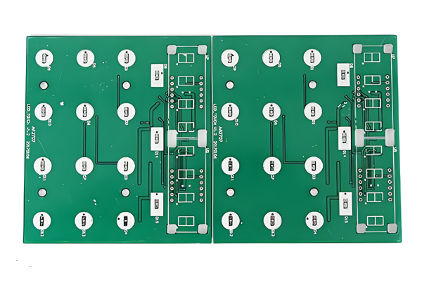
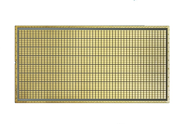
Les circuits imprimés sont des composants essentiels des appareils électroniques modernes, et le choix du nombre de couches influe directement sur les performances, la fiabilité et le coût du produit. Les appareils électroniques devenant de plus en plus complexes, les circuits imprimés multicouches (généralement 4 couches, 6 couches, 8 couches, voire plus) sont apparus pour répondre à des exigences de conception plus complexes en ajoutant des couches conductrices supplémentaires en interne.
Pourquoi les couches des circuits imprimés sont-elles toujours des nombres pairs ?
Le processus de fabrication exigeant que les feuilles de cuivre soient laminées par paires, la technologie moderne des circuits imprimés haut de gamme permet même d'intégrer des composants dans les couches internes du circuit imprimé.Cette conception innovante améliore encore l'intégration et les performances des circuits.
L'impact du nombre de couches du circuit imprimé sur les performances du produit
- Performance électrique: Un plus grand nombre de couches signifie une meilleure intégrité du signal et une meilleure compatibilité électromagnétique.
- Densité d'acheminementLes circuits complexes nécessitent plus de couches pour les interconnexions.
- Structure des coûts: L'augmentation du nombre de couches augmente considérablement les coûts de fabrication.
De l'électronique grand public aux équipements aérospatiaux, les différents domaines d'application ont des exigences très différentes en ce qui concerne le nombre de couches des circuits imprimés.Une conception raisonnable des couches peut répondre aux exigences de performance tout en contrôlant les coûts, mais un mauvais choix peut entraîner une défaillance du produit ou une escalade des coûts. Par exemple, une simple calculatrice peut ne nécessiter qu'un circuit imprimé à une seule couche, alors que les smartphones utilisent généralement 8 à 10 couches et que les cartes mères de serveurs à haute performance peuvent même atteindre 16 couches ou plus.

Facteurs clés pour déterminer le nombre de couches des circuits imprimés
La sélection du nombre de couches de PCB est un processus de prise de décision qui nécessite l’examen complet de multiples facteurs.Lorsque les clients souhaitent fabriquer des cartes de circuits imprimés, les fabricants doivent comprendre clairement les exigences des utilisateurs et fournir les recommandations correspondantes des ingénieurs afin de trouver l’équilibre optimal entre les exigences de performance et les contraintes de coût, fournissant ainsi aux clients des produits satisfaisants et un excellent service.
Champ d'application et exigences en matière de fréquence de fonctionnement
Les appareils électroniques des différentes industries ont des exigences très différentes en matière de circuits imprimés. Fréquence de fonctionnement est l'un des principaux paramètres déterminant le nombre de couches du circuit imprimé, les applications à haute fréquence nécessitant généralement plus de couches pour garantir l'intégrité du signal. Les applications à haute fréquence nécessitent généralement un plus grand nombre de couches pour garantir l'intégrité du signal :
- Électronique grand public (par exemple, écouteurs Bluetooth) :En général, cartes de 4 à 6 couches
- Équipement de télécommunications (par exemple, stations de base 5G) :Peut nécessiter 12 couches ou plus
- Électronique automobile (par exemple, unités de contrôle ECU) :Principalement 6 à 8 couches
- Systèmes aérospatiaux :10 couches ou plus pour garantir une très grande fiabilité
Les circuits haute fréquence (>120MHz) sont soumis à des exigences plus strictes en matière de nombre de couches de PCB, car l'augmentation des vitesses de transmission des signaux entraîne des risques accrus d'interférences électromagnétiques (EMI).Les circuits imprimés multicouches fournissent des plans d'alimentation et de masse dédiés, contrôlant efficacement les chemins de retour des signaux et réduisant la diaphonie et les radiations.
Évaluation de la complexité des circuits et de la densité des composants
Complexité du circuit influe directement sur les exigences en matière de nombre de couches de circuits imprimés. La complexité peut être évaluée à partir des dimensions suivantes :
- Nombre de composants :Particulièrement les dispositifs à nombre de broches élevé comme les boîtiers BGA
- Nombre de réseaux de signalisation :Nombre total d'interconnexions nécessaires
- Exigences particulières en matière de conception :Contrôle de l'impédance, paires différentielles, adaptation de la longueur, etc.
Densité des composants est une autre mesure importante, qui peut être calculée à l'aide de la formule de la densité de PIN :
Densité de PIN = Surface de la carte (in²)/(Nombre total de broches sur la carte/14)Sur la base des résultats des calculs, les valeurs empiriques suivantes peuvent être référencées :
- Placement des composants sur une seule face : La densité de PIN>1,0 peut utiliser 2 couches ; 0,6-1,0 suggère 4 couches ; <0,6 nécessite 6 couches ou plus.
- Placement de composants sur deux faces :Les normes de densité peuvent être assouplies, mais il faut tenir compte des facteurs de dissipation thermique et d'assemblage.
Considérations relatives au budget et au calendrier de fabrication
Lorsque l'on considère le nombre de couches d'un circuit imprimé, le coût de fabrication est un facteur qui ne peut être ignoré.La différence de coût entre les circuits imprimés à une ou deux couches et les circuits imprimés multicouches réside principalement dans la complexité de la conception et de la fabrication. Une plus grande capacité s'accompagne souvent d'un coût plus élevé.
En outre, il existe une relation proportionnelle entre le nombre de couches du circuit imprimé et le prix - en général, plus il y a de couches, plus les prix sont élevés.Cela s'explique principalement par le fait que les processus de conception et de fabrication des circuits imprimés multicouches sont plus complexes, ce qui augmente naturellement les coûts.Pour évaluer plus précisément les coûts des circuits imprimés, vous pouvez utiliser des sites web de devis de circuits imprimés qui aident à estimer les coûts en fonction de différents paramètres tels que le type de conducteur, la taille, la quantité et le nombre de couches. Les calculateurs en ligne peuvent également aider à sélectionner les matériaux d'isolation et les épaisseurs appropriés pour une compréhension plus complète des structures de coûts des PCB.
Délai de livraison est un autre facteur critique dans la fabrication des circuits imprimés, en particulier pour la production en grandes quantités. Les délais de livraison varient selon le nombre de couches, principalement en fonction de la surface du circuit imprimé. Un investissement accru peut parfois raccourcir les délais de livraison.
Exigences en matière de densité de broches et de couche de signaux
Le choix du nombre de couches du circuit imprimé est également étroitement lié à la densité des broches et aux besoins en matière de couches de signaux.Par exemple, une densité de broches de 0 nécessite généralement 2 couches de signaux, tandis que les densités de broches inférieures nécessitent davantage de couches.Lorsque la densité des broches atteint 2 ou moins, au moins 10 couches peuvent être nécessaires.
Méthode de sélection des couches de PCB
Dans la conception technique réelle, la sélection des numéros de couche des circuits imprimés nécessite une prise de décision scientifique basée sur les exigences spécifiques du projet et les contraintes techniques.Voici des méthodes pratiques et des règles empiriques résumées par Topfast sur la base de plus de dix ans d'expérience dans la fabrication de circuits imprimés.
Estimation du nombre de couches en fonction de la densité des broches
Densité des broches est une mesure efficace pour évaluer les exigences en matière de nombre de couches de circuits imprimés, calculée comme suit :
Densité de broches = Surface de la carte (in²)/(Nombre total de broches sur la carte/14)En fonction des résultats, se référer aux critères de sélection suivants :
Tableau : Densité des broches en fonction du nombre de couches pour le placement de composants sur une seule face
| Plage de densité des broches | Couches recommandées | Applications |
|---|---|---|
| >1.0 | 2 | Électronique grand public simple |
| 0.7-1.0 | 4 | Contrôles industriels généraux |
| 0.5-0.7 | 6 | Équipement de réseau |
| <0.5 | 8+ | Serveurs haut de gamme |
Tableau : Densité des broches en fonction du nombre de couches pour un placement double face
| Plage de densité des broches | Couches recommandées | Applications |
|---|---|---|
| >1.5 | 2 | Produits de complexité moyenne à faible |
| 1.0-1.5 | 4 | Périphériques pour smartphones |
| 0.7-1.0 | 6 | Électronique automobile |
| <0.7 | 8+ | Calcul à haute performance |
Règles empiriques concernant le rapport entre la fréquence et le nombre de couches
Fréquence du processeur est un autre élément clé, les circuits à haute fréquence nécessitant généralement plus de couches pour l'intégrité du signal :
- 50MHz: Généralement suffisant avec 2 couches
- 50- 120MHz: Recommander 4 couches (signal-masse-alimentation-signal)
- 120MHz-1GHz6 couches (meilleur rapport coût/performance)
- >1GHz: Nécessite 8+ couches avec une analyse SI stricte
Cas particuliers où un plus grand nombre de couches est nécessaire malgré des fréquences plus basses :
- Plusieurs domaines de tension (≥3 alimentations indépendantes)
- Interfaces série à haut débit (PCIe, USB3.0+)
- Circuits analogiques sensibles (ADC/DAC de haute précision)
Stratégies relatives au type de mémoire et au nombre de couches
Sous-système mémoire influencent de manière significative le nombre de couches du circuit imprimé :
Systèmes de mémoire statique:
- SRAM/Flash NOR parallèle : 2 couches peuvent suffire
- Point clé : Assurer la stabilité de l'alimentation
Systèmes de mémoire dynamique:
- SDRAM/DDR : 4 couches au minimum
- DDR2/3 : 6 couches recommandées (avec plans de référence dédiés)
- DDR4/5 : nécessite plus de 8 couches avec une correspondance stricte des longueurs.
Systèmes NAND Flash:
- NAND conventionnelle : 4 couches suffisantes
- eMMC/UFS : Déterminé par la fréquence (typiquement 6 couches)
Emballage BGA et adaptation du nombre de couches
Dispositif BGA l'emballage a une incidence directe sur le nombre de couches du circuit imprimé :
Distance entre les broches et le nombre de couches:
- Pas ≥1,0 mm : 2 couches peuvent fonctionner
- Pas de 0,8 mm : Suggère 4 couches
- Pas de 0,65 mm :6 couches recommandées
- Pas ≤0,5mm :Nécessite 8+ couches
Lignes directrices sur le nombre de broches:
- 100 broches : Envisager moins de couches
- 100-300 broches :Couches standard recommandées
- >300 pins :Ajouter 1 à 2 couches
Types de BGA spéciaux:
- BGA à puce : ajouter 2 couches
- BGA à pas ultrafin (≤0,4mm) : Nécessite la technologie HDI
Considérations sur le nombre de couches spécifiques à l'industrie
Les différentes industries ont des exigences particulières qui influent sur le nombre de couches :
Électronique automobile:
- De base : 4 couches au minimum (fiabilité)
- Groupe motopropulseur : 6 couches + matériaux haute température
- Systèmes ADAS : 8 couches + matériaux à haute fréquence
Dispositifs médicaux:
- Équipement de diagnostic : 6 couches (faible bruit)
- Dispositifs implantables :4 couches (miniaturisation)
Contrôles industriels:
- Automate standard : 4 couches
- Contrôle des mouvements : 6 couches (résistance EMI)
Electronique grand public:
- Produits portables : 4 couches (miniaturisation)
- Maison intelligente :Varie selon la fonctionnalité
Optimisation des coûts et compromis sur le nombre de couches
En cas de pression budgétaire, il convient de prendre en compte les éléments suivants stratégies d'optimisation du nombre de couches:
- “Pseudo-multi-layer” design:
- Utiliser 2 couches + cavaliers pour simuler une fonctionnalité multicouche
- Convient aux conceptions à basse fréquence et à faible densité
- Technologie de laminage hybride:
- Augmentation locale des couches (par exemple, sous les zones BGA)
- Équilibre entre coût et performance
- Empilement asymétrique de couches:
- Réduire les couches de signaux tout en conservant les plans d'alimentation et de masse
- Par exemple, carte à 6 couches en configuration 1-2-2-1
- IDH substitution technologique:
- Utiliser des interconnexions à haute densité pour réduire le nombre total de couches
- Idéal pour les conceptions à grand nombre de broches mais à petite surface
En tenant compte de tous les facteurs susmentionnés ainsi que des exigences et des contraintes spécifiques du projet, les ingénieurs peuvent procéder à des sélections scientifiquement fondées du nombre de couches du circuit imprimé, qui permettent d'équilibrer de manière optimale les performances, la fiabilité et le coût.
Foire aux questions (FAQ)
Au cours du processus de sélection des numéros de couche des circuits imprimés, certains problèmes et confusions typiques sont souvent rencontrés. Des réponses professionnelles sont apportées à ces questions courantes.
Comment déterminer si une conception nécessite plus de couches de PCB ?
Plusieurs indicateurs clairs suggèrent la nécessité de augmenter le nombre de couches du circuit imprimé:
- Achèvement insuffisant de l'acheminement:
- Impossible de terminer l'acheminement après avoir atteint 90%
- Utilisation intensive de cavaliers pour résoudre les problèmes de croisements
- Problèmes d'intégrité du signal:
- Les signaux critiques présentent une forte sonnerie
- Échec des tests de diagramme de l'œil
- Le taux d'erreur binaire du système dépasse les limites
- Problèmes de stabilité de l'alimentation:
- Les fluctuations de tension dépassent les tolérances
- Bruit de commutation simultanée perceptible (SSN)
- Échecs des essais CEM:
- Les émissions rayonnées dépassent les normes
- Tests d'immunité infructueux
- Difficultés de gestion thermique:
- La surchauffe locale ne peut être résolue avec les couches actuelles
- Nécessité de couches thermiques ou de vias supplémentaires
Méthodes de vérification pratiques:
- Le contrôle des règles de conception (DRC) révèle de nombreuses violations
- La vue en 3D révèle des itinéraires extrêmement encombrés
- L'analyse de simulation indique que les paramètres critiques ne sont pas respectés
Quels sont les problèmes potentiels liés à l'augmentation du nombre de couches de circuits imprimés ?
Si l'ajout de couches permet de résoudre de nombreux problèmes de conception, il peut aussi en introduire d'autres. nouveaux problèmes:
- Augmentation des coûts:
- Augmentation du coût de 30 à 50 % par 2 couches supplémentaires
- Augmentation des dépenses d'ingénierie non récurrentes (NRE)
- Baisse des rendements de production:
- Difficulté accrue dans l'alignement des couches
- Taux de défectuosité de la couche interne plus élevés
- Délais d'exécution prolongés:
- 3-5 jours supplémentaires par 2 couches additionnelles
- Options limitées pour l'expédition d'urgence
- Difficultés de réparation:
- Difficile de détecter les défauts de la couche interne
- Diminution des taux de réussite des reprises
- Augmentation du poids et de l'épaisseur:
- Impact sur la conception des appareils portables
- Peut dépasser les limites mécaniques
Stratégies d'atténuation:
- Utiliser des conceptions de couches échelonnées (nombre de couches variable selon la zone)
- Adopter l'IDH pour réduire le nombre total de couches requises
- Optimiser les empilages pour améliorer les rendements
Comment équilibrer le coût et la performance pour un nombre de couches optimal ?
Méthodes d'équilibrage coût-performance:
- Approche de vérification par étapes:
- Commencer les prototypes avec moins de couches
- Décider s'il faut ajouter des couches en fonction des résultats des tests
- Analyse du chemin critique:
- Identifier les chemins de signaux les plus critiques
- Ajouter des couches uniquement pour ces sections
- Matrice d'évaluation des coûts et bénéfices:
| Option de calque | Score de performance | Score de coût | Valeur composite |
|---|---|---|---|
| 4 couches | 70 | 90 | 78 |
| 6 couches | 85 | 70 | 80 |
| 8 couches | 95 | 50 | 75 |
- Approche modulaire de la conception:
- Les modules de base utilisent des
- Les circuits périphériques utilisent un système à deux couches
Règles pratiques:
- Produits de consommation : ≤6 couches
- Équipement industriel : 4-8 couches idéales
- Matériel de mise en réseau : 6 à 12 couches en général
- Informatique haut de gamme : 12+ couches
Quelles sont les applications typiques des différents nombres de couches des circuits imprimés ?
Applications caractéristiques par nombre de couches :
2 couches:
- Tableaux de commande des appareils
- Circuits de puissance simples
- Modules industriels de base
- Jouets électroniques
4 couches:
- Smartphones
- Routeurs
- Calculateurs automobiles
- Moniteurs médicaux
6 couches:
- Cartes graphiques haut de gamme
- Automates industriels
- Commutateurs de réseau
- Contrôleurs de drone
8 couches:
- Cartes mères de serveurs
- Stations de base 5G
- ADAS avancés
- Instruments de test haut de gamme
10+ couche:
- Supercalculateurs
- Électronique aérospatiale
- Systèmes radar haut de gamme
- Plans d'appui complexes
Idées fausses courantes dans la sélection du nombre de couches des circuits imprimés
- “Plus il y a de couches, mieux c'est” ;.:
- Fait : la sur-ingénierie entraîne un gaspillage des coûts
- Vérité : Répondre aux besoins de manière adéquate
- “2-layer can’t do high-speed” ;:
- Fait : il est possible de réaliser des circuits simples à grande vitesse
- La vérité : Nécessite une conception minutieuse
- “Les plans d'alimentation doivent être solides.” ;:
- Fait : Les avions fractionnés peuvent être plus efficaces
- Vérité : En fonction des besoins actuels
- “Les signaux de la couche interne sont plus faibles” ;:
- Fait : les signaux internes sont plus stables
- Vérité : Affecté par les plans de référence
- “L'ajout de couches résout toujours le problème de l'EMC.” ;:
- Fait : des empilages de mauvaise qualité peuvent aggraver la CEM
- Vérité : la conception des piles est plus critique
Pratiques correctes:
- Baser les décisions sur les exigences du système
- Valider par des simulations
- Consulter les conseils du fabricant de la carte de circuit imprimé.
- Référence à des conceptions similaires réussies
Lecture associée
Quand faut-il choisir un circuit imprimé à 2 couches ou à 4 couches ?


Articles connexes