Processus d'assemblage des circuits imprimés
Table des matières
Qu'est-ce que le processus d'assemblage des circuits imprimés ?
Assemblage du circuit imprimé (Printed Circuit Board Assembly, PCBA) est le processus de fabrication complet qui consiste à monter des composants électroniques sur des cartes de circuits imprimés. Cette procédure complexe et précise comporte de nombreuses étapes critiques, notamment l'impression de pâte à braser, le placement des composants, le soudage par refusion, l'inspection de la qualité et bien d'autres encore, pour finalement transformer des cartes nues en assemblages électroniques entièrement fonctionnels. Les produits électroniques étant de plus en plus miniaturisés et performants, les processus modernes d'assemblage de circuits imprimés doivent répondre à des exigences de plus en plus strictes en matière de précision et de fiabilité.
7 étapes clés du processus d'assemblage des circuits imprimés
1. Impression de la pâte à braser : La première étape cruciale pour la précision
L'impression de la pâte à braser est l'étape principale et la plus fondamentale de l'assemblage des circuits imprimés.Semblable à la sérigraphie mais nécessitant une plus grande précision, ce processus utilise des pochoirs en acier inoxydable (généralement d'une épaisseur de 0,1 à 0,15 mm).
Analyse de la composition de la pâte à braser:
Les pâtes à braser modernes sans plomb sont généralement composées de.. :
- 96,5% Etain (Sn)
- 3 % Argent (Ag)
- 0,5 % Cuivre (Cu)
Cette combinaison d'alliages offre d'excellentes performances de brasage et de résistance mécanique. La pâte contient également du flux, qui élimine les couches d'oxyde des surfaces métalliques, réduit la tension superficielle de la soudure et favorise l'écoulement et le mouillage de la soudure.
Processus d'impression de précision:
- Le circuit imprimé est fixé sur la table de l'imprimante à l'aide de fixations de précision.
- Le pochoir et les pastilles du circuit imprimé sont alignés avec précision (typiquement contrôlés dans une tolérance de ±25μm).
- La raclette se déplace à un angle approprié (généralement 60°) et exerce une pression (environ 5-10 kg) pour pousser la pâte à souder à travers les ouvertures du pochoir.
- Lors du démoulage, le pochoir se sépare du circuit imprimé, ne laissant de la pâte que sur les pastilles.
Points de contrôle de la qualité:
- Cohérence de l'épaisseur de la pâte à braser (mesurée à l'aide d'une jauge d'épaisseur laser)
- Précision de la position d'impression
- Absence de pontage, de soudure insuffisante ou de pointes
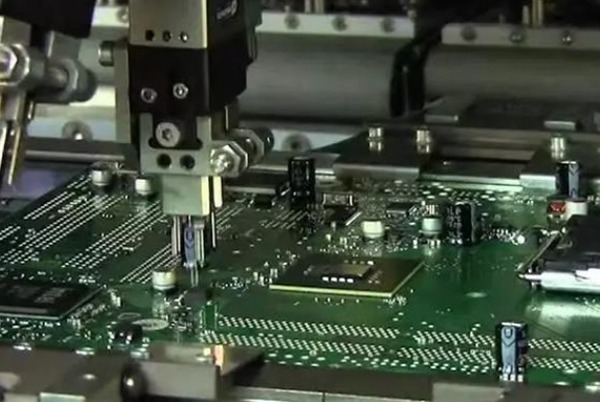
2.Placement de composants SMT :Précision à grande vitesse “Pick and Place” ;
Après l'impression de la pâte à braser, le circuit imprimé entre dans la ligne de production de la technologie de montage en surface (SMT), où des machines de placement à grande vitesse positionnent les composants avec précision.
Technologie moderne des machines de placement:
- Précision de placement : ±25μm (les équipements haut de gamme peuvent atteindre ±15μm).
- Vitesse de placement : 30 000-150 000 composants par heure
- Taille minimale des composants : Peut prendre en charge des boîtiers 01005 (0,4×0,2 mm) ou plus petits.
Déroulement du processus de placement:
- Système d'alimentation : Composants fournis par ruban, tubes ou plateaux
- Alignement par vision :Des caméras à haute résolution identifient les marques fiduciaires des circuits imprimés
- Collecte des composants :Des buses à vide collectent les composants dans les chargeurs.
- Inspection des composants :Certaines machines sont équipées de caméras permettant de vérifier la polarité, les dimensions, etc.
- Placement précis :Les composants sont placés sur la pâte à braser selon des coordonnées programmées.
Facteurs d'influence clés:
- Précision de l'alimentation en composants
- Sélection et entretien des buses
- État de l'étalonnage de la machine
- Contrôle de l'environnement (typiquement 23±3°C, 40-60% RH)
3.Soudure par refusion :Le profil de température détermine la qualité de la soudure
Le brasage par refusion est le processus critique qui permet de faire fondre la pâte à braser pour former des connexions électriques fiables, ce qui nécessite un contrôle précis du profil de température.
Profil de température de refusion typique:
- Zone de préchauffage : Montée en puissance à 1-3°C/s jusqu'à 150-180°C (activation du flux)
- Zone de trempage :Maintenir une température de 140-180°C pendant 60-90 secondes (égalise la température des PCB/composants).
- Zone de refusion :Chauffage rapide jusqu'à la température maximale de 235-245°C (maintenu pendant 30-60 secondes)
- Zone de refroidissement :Refroidissement contrôlé inférieur à 4°C/s (évite les chocs thermiques)
Comparaison des types de fours de refusion:
- Four à convection : Meilleure uniformité, convient aux circuits imprimés complexes
- Four à infrarouge :Efficacité de chauffage élevée, mais risque d'effets d'ombre
- Four à phase vapeur :Excellente uniformité mais coût plus élevé, principalement pour les produits militaires.
Manipulation spéciale des circuits imprimés double face:
Pour les circuits imprimés SMT double face, il convient généralement de souder d'abord le côté où se trouvent les composants les plus légers. Lors de la deuxième refusion, assurez-vous que les composants précédemment soudés peuvent supporter la température.
4.Inspection de la qualité :Des défenses multiples pour garantir la fiabilité
Après le soudage, les circuits imprimés sont soumis à des contrôles de qualité rigoureux, notamment :
4.1 Inspection visuelle manuelle
- Applications : Production de faibles volumes, vérification des retouches
- Vérifie :Composants manquants ou erronés, inversion de la polarité, défauts de soudure évidents.
- Limites :Faible efficacité, tendance à la fatigue, seulement des articulations visibles
4.2 Inspection optique automatisée (AOI)
- Principe : Des caméras multi-angles à haute résolution comparent des échantillons d'or.
- Capacités :Volume de soudure, pontage, désalignement des composants
- Avantages :Rapide (généralement 3 à 10 secondes par planche), cohérent
- Spécifications :Résolution de 20μm, <5% de taux de fausse alarme.
4.3 Inspection par rayons X (AXI)
- Applications : BGA, QFN et autres joints cachés
- Capacités :Intégrité des billes de soudure, vides, alignement des couches
- Systèmes :Rayons X 2D (coût réduit), Rayons X 3D (tomographie)
Contrôle statistique des processus (CSP):
Les usines modernes de PCBA transmettent les données d'inspection en temps réel, en utilisant des méthodes SPC pour contrôler la stabilité du processus et prévenir les défauts de lot.
5.Assemblage de composants à trous traversants :La technologie traditionnelle dans les applications modernes
Bien que la technologie SMT domine, de nombreux circuits imprimés nécessitent encore des composants THT (Through-Hole Technology), en particulier des connecteurs et des dispositifs de haute puissance.
Deux principales méthodes de soudage:
5.1 Soudure à la vague
- Processus : Insertion→ fixation de la colle→ soudure à la vague→ nettoyage
- Types de vagues :Vague simple (vague λ), vague double (turbulente+plate)
- Température :Pot de soudure maintenu à 250-260°C
- Applications :Cartes à technologie mixte à volume élevé et à une seule face
5.2 Soudure sélective
- Principe : Brasage localisé pour des trous de passage spécifiques
- Avantages :Impact thermique minimal, idéal pour les panneaux double face
- Variantes :Brasage au laser, micro-ondes, robots de brasage
L'essentiel de la soudure à la main:
- Contrôle de la température : 300-350°C en fonction de la taille des composants
- Durée : 2 à 3 secondes par articulation pour éviter les dégâts
- Volume de soudure : Former des filets coniques d'environ 45
6.Essais fonctionnels :Vérification de la conformité de la conception
L'essai fonctionnel est le dernier point de contrôle de la qualité, validant les performances du produit.
Méthodes d'essai courantes:
6.1 Essai en circuit (ICT)
- Utilise un "lit de clous" pour contacter les points de test
- Vérifie : les courts-circuits, les ouvertures, les valeurs des composants, les fonctions de base
- Avantages :Localisation précise des défauts, essais rapides
6.2 Essai du circuit fonctionnel (ECF)
- Simule les conditions de fonctionnement réelles
- Introduit des signaux d'essai, vérifie les sorties
- Peut s'intégrer à l'automatisation pour des tests à 100 %.
6.3 Test de balayage des frontières
- Pour les PCB à haute densité et inaccessibles
- Utilise l'interface JTAG
- Idéal pour les dispositifs programmables (FPGA, CPLD)
Analyse de la couverture des tests:
D'excellents plans de test doivent couvrir plus de 90 % des modes de défaillance potentiels, optimisés par l'analyse des modes de défaillance et de leurs effets (AMDE).
7.Nettoyage et protection :Les clés de la longévité des produits
Les exigences de fiabilité élevées de l'électronique moderne rendent le nettoyage de plus en plus critique.
Options de nettoyage:
7.1 Nettoyage aqueux
- Utilise de l'eau déionisée (résistivité >1MΩ-cm)
- Possibilité d'ajouter des produits de nettoyage respectueux de l'environnement
- Convient à la plupart des appareils électroniques conventionnels
7.2 Nettoyage au solvant
- Utilise des solvants à base d'alcool ou d'hydrocarbures
- Forte capacité de nettoyage, séchage rapide
- Nécessite des précautions en matière de sécurité et d'environnement
7.3 Processus sans nettoyage
- Utilise une pâte à souder sans nettoyage et à faible teneur en résidus
- Doit toujours répondre aux normes de propreté ionique (<1,56μg/cm² équivalent NaCl).
Revêtement conforme:
Pour les applications en environnement difficile :
- Acrylique : Facile à appliquer et à retravailler
- Polyuréthane : excellente résistance chimique
- Silicone : Performance supérieure à haute température
Tendances modernes en matière d'assemblage de circuits imprimés
Technologie d'interconnexion à haute densité (HDI)
- Lignes plus fines (<50μm)
- Technologie des microvia (vias aveugles/enfouis)
- Interconnexion de toutes les couches
Fabrication d'électronique flexible
- Assemblage de substrats flexibles
- Montage sur surface courbe en 3D
- Circuits électroniques étirables
Transformation de la fabrication intelligente
- Applications des jumeaux numériques
- Inspection de la qualité alimentée par l'IA
- Systèmes de production adaptatifs
Exigences en matière de fabrication écologique
- Matériaux sans plomb et sans halogène
- Procédés économes en énergie
- Recyclage des déchets
Problèmes courants liés à l'assemblage des circuits imprimés et solutions
| Type de problème | Causes potentielles | Solutions |
|---|---|---|
| Ponts de soudure | Mauvaise conception du pochoir, excès de pâte | Optimiser les ouvertures du pochoir, ajuster les paramètres d'impression |
| Joints de soudure à froid | Faible activité de la pâte, profil inapproprié | Modifier la pâte, optimiser la courbe de refusion |
| La mise au tombeau | Conception asymétrique du coussin, chauffage inégal | Optimiser la conception des tampons, ajuster la refusion |
| Boules de soudure | Pâte oxydée, humidité élevée | Contrôler l'humidité, réduire l'exposition à la pâte |
| Vides dans les BGA | Dégazage de la pâte, chauffage rapide | Sélectionner une pâte à faible viscosité, optimiser le préchauffage |
Conclusion
L'assemblage de circuits imprimés est le processus de fabrication essentiel qui transforme les conceptions en produits physiques, intégrant la science des matériaux, la mécanique de précision, l'automatisation et bien d'autres choses encore. L'électronique devenant de plus en plus complexe, les processus modernes d'assemblage de circuits imprimés évoluent vers plus de précision, d'efficacité et d'intelligence. La maîtrise de l'ensemble du processus d'assemblage et des points de contrôle clés est essentielle pour garantir la qualité et la productivité. Qu'il s'agisse d'un faible volume, d'un mélange élevé ou d'une production de masse, la sélection des itinéraires de processus et des méthodes de qualité appropriés en fonction des caractéristiques du produit reste fondamentale.


Articles connexes