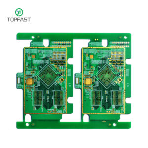
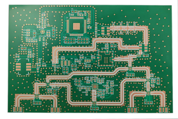
Description
In today’s rapidly evolving fields of wireless communication, 5G technology, and automotive electronics, high-frequency PCBs have become a critical factor in enhancing the performance of electronic devices. Topfast is a high-frequency PCB manufacturer with 17 years of professional experience, offering customers a one-stop high-frequency circuit solution from design to production through advanced material selection, precision manufacturing processes, and strict quality control.
Table of Contents
Core Technical Advantages of High-Frequency PCBs
The fundamental difference between high-frequency PCBs and traditional circuit boards lies in their superior signal processing capabilities and stability. Topfast’s high-frequency PCB products feature the following core technical advantages:
1. Ultra-Low Loss Signal Transmission
Utilizing PTFE (polytetrafluoroethylene) substrate material and modified ceramic-filled composite materials, we ensure the dielectric constant (Dk) remains stable within the range of 2.2–3.5, with a loss factor (Df) below 0.005 at 10 GHz. This ultra-low loss characteristic enables our high-frequency PCBs to perform exceptionally well in applications such as 5G base stations and millimeter-wave radar, achieving signal transmission efficiency improvements of over 40% compared to standard FR-4 materials.
Notably, our high-frequency PCBs achieve insertion loss of less than 0.1 dB/inch in 77 GHz automotive radar applications, ensuring the radar system maintains precise target detection capabilities even in complex environments.
2. Precise Impedance Control and Signal Integrity
Using advanced mSAP (modified semi-additive process) technology, differential trace width tolerance is controlled within ±8% (@100Ω impedance). Back drilling technology (depth control accuracy ±25μm) effectively eliminates stub effects, minimizing signal reflection. Impedance control accuracy of ±5% is achieved within the 50GHz frequency range, meeting the most stringent requirements for high-speed signal transmission. For example, in 56Gbps SerDes applications, the PCB maintains signal integrity, keeping jitter below 0.01UI.
3. Exceptional Environmental Adaptability
High-frequency PCBs utilize special materials and processing techniques, offering outstanding environmental stability:
Water absorption rate <0.02% (far below FR-4’s 0.1%), suitable for high-humidity environments
Resistant to acid and alkali corrosion, compliant with the stringent IPC-4103 standard
Dielectric constant temperature coefficient <50 ppm/°C (-40°C to 150°C range)
Passes 1,000 thermal cycle tests (-55°C to 125°C)
These characteristics enable PCB products to meet the demanding application requirements of aerospace, automotive electronics, and other harsh environments.
Topfast High-Frequency PCB Manufacturing Process
1. Special Material Processing Technology
We have established long-term partnerships with internationally renowned high-frequency material suppliers and mastered precision processing technologies for various high-frequency materials:
1. PTFE Material Processing
We use a stepwise temperature ramping curve (peak temperature 280±5°C) and vacuum hot pressing process (pressure 30-50 kg/cm²) to effectively control PTFE phase transitions and ensure lamination quality.
2. Ceramic Substrate Processing
For aluminum oxide (Al₂O₃) and aluminum nitride (AlN) substrates, we employ laser direct writing technology to achieve 50μm line width precision, meeting high-density interconnect requirements.
3. Hybrid Pressing Technology
For PTFE and FR-4 hybrid designs, we use specialized adhesive sheets such as RO4450B and optimize pressing parameters to address mismatched thermal expansion coefficients (CTE) between different materials.
2. Precision Micro-processing Capabilities
Topfast has invested heavily in advanced processing equipment to establish a comprehensive precision processing system:
UV Laser Drilling: Minimum hole diameter of 75μm, positional accuracy of ±15μm
Picosecond Laser Cutting: Edge roughness Ra<5μm, reducing edge effects on high-frequency signals
Plasma treatment: Utilizes a CF4/O2 mixed gas to activate the PTFE surface, ensuring interlayer bonding strength
3. Multi-layer interconnection process innovation
For high-frequency multi-layer board manufacturing, Topfast has developed a series of innovative processes:
1. High-precision layer alignment: Utilizes a CCD automatic alignment system to achieve interlayer alignment deviation <25μm
2. Low-loss interconnects: Optimizing via design and copper plating processes to control via insertion loss below 0.05 dB at 10 GHz
3. Signal integrity protection: Employing a unique “ground hole shielding” design to effectively suppress interlayer crosstalk, keeping crosstalk levels below -50 dB
Strict Quality Control System
Topfast has established a comprehensive quality control system throughout the entire production process to ensure that every high-frequency PCB meets the highest standards:
1. Raw Material Control
100% incoming inspection of high-frequency substrates, including Dk/Df testing, thermal expansion coefficient measurement, etc.
Copper foil is selected from ultra-low profile (HVLP) types, with surface roughness Rz < 2 μm
2. Process Control
Online TDR (Time Domain Reflectometer) impedance testing ensures control accuracy within ±5%
Infrared thermal imaging cameras detect lamination defects with a resolution of 0.1°C
Cross-section analysis is conducted for each batch to monitor hole wall quality and plating uniformity
3. Reliability Verification
1,000 thermal cycle tests (-55°C to 125°C)
85°C/85% RH high-temperature and high-humidity tests (1,000 hours)
Thermal shock tests (-65°C to 150°C, 500 cycles)
High-frequency PCB products have obtained UL safety certification, IPC Class 3 standards, and ISO 9001:2015 quality management system certification, with their quality and reliability widely recognized by the industry.
Application Cases and Industry Solutions
1.5G Communication Field
Topfast provides high-frequency PCB solutions for 5G base station AAUs (active antenna units):
Using Rogers RO4835 material to achieve Dk=3.48±0.05 stability
Developing a special antenna array design, improving beamforming accuracy by 30%
Optimizing thermal design to ensure temperature rise <15°C at 40W power
A well-known communication equipment manufacturer adopted our solution, resulting in a 20% improvement in 5G base station RF performance and a 15% increase in product yield.
2. Automotive Electronics Field
For 77GHz automotive radar applications, we offer:
Ultra-low loss PCB (Df<0.002@77GHz)
Precise microstrip line design with phase consistency <2°
Vibration-resistant design passing automotive-grade reliability testing
Our high-frequency PCBs have been applied in the ADAS systems of several leading automotive manufacturers, maintaining stable performance under extreme temperatures (-40°C to 105°C).
3. Medical Device Sector
High-frequency PCBs developed for medical radiofrequency ablation devices feature:
Precise energy control capability, enabling ±1°C temperature control
Localized energy delivery to protect healthy tissue
Compliance with medical device EMC and safety standards
Why choose Topfast?
As a high-frequency PCB manufacturer with 17 years of professional experience, Topfast has become the preferred partner in the global electronics manufacturing industry thanks to its deep technical expertise and strict quality management. We not only provide high-quality high-frequency PCB products but also offer customers comprehensive solutions throughout the entire process, from material selection and design optimization to production and manufacturing.
Whether it’s 5G communications, automotive radar, or aerospace applications, Topfast leverages its professional technical capabilities and reliable product quality to help clients achieve success in the rapidly evolving electronics industry. We look forward to collaborating with you to drive innovation and advancement in high-frequency electronic technology.