Conceção e fabrico de placas de circuito impresso de 6 camadas
Índice
Introdução às placas de circuito impresso de 6 camadas
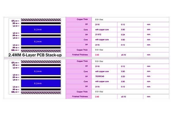
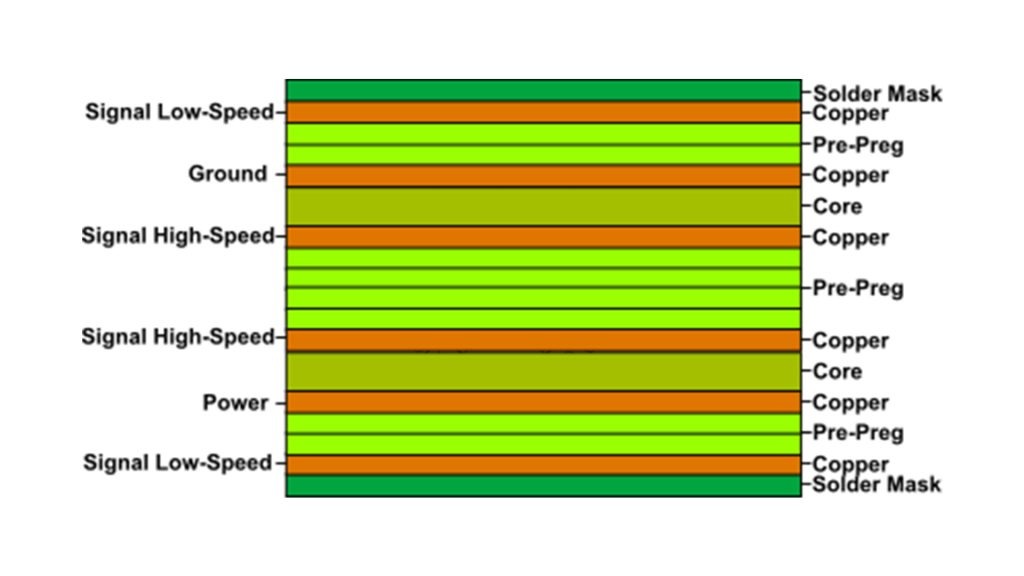
Uma placa de circuito impresso de seis camadas é uma placa de circuito impresso multicamada constituída por seis camadas alternadas de folha de cobre condutora e material isolante. Este design inovador é espantoso! Permite a criação de circuitos complexos através de uma tecnologia precisa de ligação de camadas internas, tornando-a ideal para dispositivos electrónicos de elevado desempenho. Inclui camadas de sinal, camadas de alimentação e camadas de terra. Estas camadas são dispostas da melhor forma para que a integridade do sinal e a compatibilidade electromagnética sejam optimizadas.
As placas de 6 camadas são simplesmente fantásticas!Oferecem mais espaço de encaminhamento e melhores capacidades de supressão de ruído do que as placas de quatro camadas.Isto torna-as perfeitas para circuitos digitais de alta velocidade, comunicações RF e outras aplicações.
A Topfast utiliza uma tecnologia avançada de microvia e processos de laminação de precisão para garantir a elevada fiabilidade e estabilidade das placas de seis camadas.
Vantagens das placas de circuito impresso de 6 camadas
| Vantagem | Descrição |
|---|---|
| Roteamento de alta densidade | A tecnologia Microvia permite uma disposição mais fina dos traços, poupando espaço |
| Excelente integridade de sinal | Os planos de alimentação/terra dedicados reduzem a diafonia e melhoram o desempenho de alta frequência |
| Gestão térmica superior | Vias térmicas e camadas de cobre distribuem o calor uniformemente |
| Estabilidade mecânica melhorada | Uma estrutura multicamada melhora a resistência à flexão e à vibração |
| Flexibilidade de conceção | Suporta vias cegas/enterradas para requisitos de circuitos complexos |
Topfast’s Os PCBs de 6 camadas apresentam designs de empilhamento otimizados para reduzir ainda mais a perda de transmissão, atendendo aos requisitos rigorosos para aplicações 5G e IA.
Materiais comuns & Propriedades
FR-4 Epoxy: Económica, adequada para a maioria dos produtos electrónicos de consumo, suportando 130-140°C.
Materiais de alta frequência (por exemplo, Rogers RO4350B): Baixa perda dieléctrica, ideal para estações de base 5G e sistemas de radar.
Materiais de elevado TG (TG170+): Resistente ao calor, ideal para sistemas de controlo automóvel e industrial.
Núcleo metálico (alumínio): Excelente condutividade térmica, utilizada em iluminação LED e módulos de potência.
Topfast oferece personalização total do material para corresponder precisamente às suas necessidades de desempenho.
Processos de fabrico principais
- Perfuração a laser: Os lasers UV criam microvias de 50-100μm com uma precisão de ±10μm
- Via Enchimento & Chapeamento: O revestimento por impulsos garante uma espessura uniforme do cobre, eliminando os vazios
- Controlo da laminação: A prensagem sob vácuo evita a delaminação, com expansão do eixo Z <3%
- Controlo de impedânciaTolerância de ±5% para integridade de sinal de alta velocidade
- Acabamentos de superfícieMúltiplas opções, incluindo ENIG, prata de imersão e OSP
A Topfast opera salas limpas de classe 10000 com linhas de produção totalmente automatizadas, alcançando taxas de rendimento de 99,2%.
Principais áreas de aplicação
- Equipamento de telecomunicações: Circuitos RF para estações de base 5G/módulos ópticos
- Eletrónica automóvelUnidades de controlo ADAS, sistemas de info-entretenimento
- Controlos industriais: Placas principais de PLC, servo-accionamentos
- Dispositivos médicosUnidades de processamento de imagens médicas
- Eletrónica de consumoRouters topo de gama, consolas de jogos
A Topfast forneceu soluções de PCB de 6 camadas para mais de 500 clientes globais com uma capacidade anual superior a 500,000㎡.
Problemas comuns e soluções
Questão 1: Desalinhamento das camadas
Solução: O sistema de posicionamento de perfuração por raios X atinge uma precisão de registo de ±25μm
Questão 2: Perda de sinal de alta frequência
Solução: Cobre de perfil ultra-baixo (RTF/VLP) com designs híbridos de empilhamento
Questão 3: Delaminação pós-solda
Solução: Pré-cozedura + materiais de alto TG melhoram a resistência ao ciclo térmico 3x
Questão 4: Incompatibilidade de impedância
Solução: Monitorização dieléctrica em tempo real + algoritmos de compensação adaptativos
A Topfast fornece suporte técnico de ponta a ponta, desde o projeto até a produção em massa.
Sobre a Topfast
Como um fabricante de PCB premium, a Topfast é especializada em placas de 6+ camadas com 17 anos’ experiência, apresentando:
- Sistemas alemães de perfuração a laser LPKF
- Equipamento de inspeção AOI Orbotech israelita
- Medidores de impedância MKS americanos
- IATF16949/ISO13485 certifications
Contacte os nossos engenheiros hoje mesmo para obter soluções personalizadas de PCB de 6 camadas!


Publicações relacionadas