Como são feitas as telas de seda para PCB?
Índice
1. O que é serigrafia em PCB?
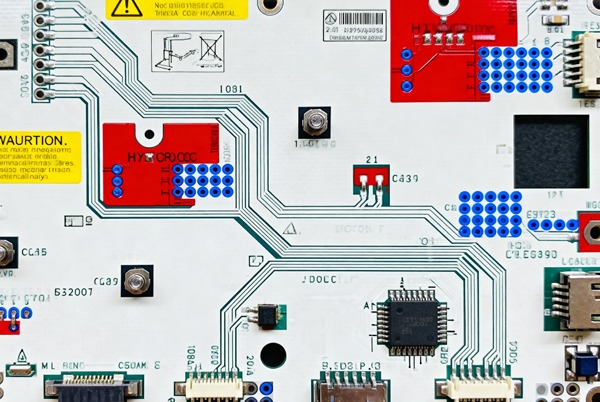
A serigrafia PCB é a camada que contém texto e marcações simbólicas numa placa de circuito impresso, aplicada utilizando tecnologia de serigrafia com tinta de resina epóxi na superfície da PCB. Estas marcações incluem informações cruciais, tais como identificadores de componentes, indicadores de polaridade e informações de versão, fornecendo referências essenciais para Montagem de PCB, testes e reparação.
2. Valor fundamental da serigrafia em PCB
- Melhora a eficiência da montagem: Designadores de componentes claros e marcações de polaridade reduzem erros de soldagem.
- Facilita a depuração e o reparoIdentificadores claros aceleram o processo de resolução de problemas.
- Melhora a rastreabilidade do produto: Números de versão, códigos de data e outras informações melhoram o sistema de gestão da qualidade.
- Exibição da imagem da marca: Os logótipos da empresa e as marcas de certificação aumentam o profissionalismo do produto.
3. Informações importantes contidas na serigrafia do PCB
3.1 Marcações essenciais
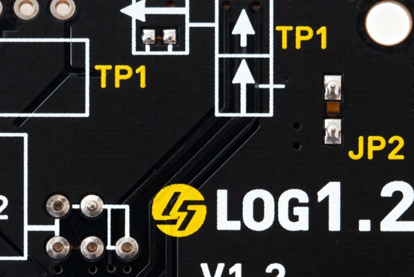
- Designadores de referência dos componentes: Como R1, C5, U3, etc.
- Marcações de polaridade: Indicadores de ânodo/cátodo para componentes como díodos e condensadores eletrolíticos.
- Marcador do pino 1: Indica o pino inicial para circuitos integrados.
- Descrição dos componentes: Caixa delimitadora de componentes complexos
- Identificadores de pontos de teste: Marque os locais de teste dos sinais principais.
3.2 Marcações informativas
- Logótipo da empresa e informações sobre direitos autorais
- Número da versão da PCB e código da data
- Informações do fabricante e número de série
- Marcas de certificação de segurança (UL, CE, RoHS, etc.)
- Símbolos de aviso e notas especiais de operação
4. Fluxo do processo de produção de serigrafia de PCB
4.1 Fase de projeto
Especificações de configuração da ferramenta EDA:
- Defina a camada de serigrafia separadamente como a camada de serigrafia superior/inferior.
- Seleção de fonte: Use fontes Sans-serif padrão.
- Tamanhos padrão: Altura 25-35 mil, largura da linha 5 mil.
- Configuração de cores: Branco é a cor principal; amarelo, preto ou vermelho para necessidades especiais.
Pontos-chave do design:
- Evite a sobreposição da serigrafia com almofadas ou vias.
- Mantenha uma orientação uniforme dos caracteres (da esquerda para a direita, de baixo para cima).
- Use linhas-guia para anotações em áreas de alta densidade.
- Certifique-se de que as marcações dos componentes de polaridade estejam claras e bem visíveis.
4.2 Comparação dos três principais processos de produção
4.2.1 Serigrafia tradicional
Fluxo do processo:
Preparação da moldura → Esticar a malha → Revestir com emulsão fotossensível → Exposição → Revelação → Impressão → Cura
Vantagens: Baixo custo, alta eficiência, adequado para produção em grande volume.
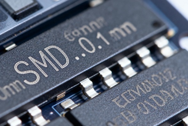
Limitações: Precisão limitada (largura mínima da linha > 0,15 mm), não adequado para placas de alta densidade.
4.2.2 Imagem fotográfica líquida (LPI)
Fluxo do processo:
Máscara de solda líquida fotoimageável → Exposição UV → Revelação → Cura
Vantagens: Alta resolução (até 0,1 mm), boa planicidade.
Aplicações: Placas PCB com requisitos de precisão média.
4.2.3 Impressão direta de legendas (DLP)
Fluxo do processo:
Acionamento direto a partir de dados CAD → Impressão a jato de tinta → Cura UV
Vantagens: Máxima precisão (até 0,05 mm), fluxo de trabalho digital, adequado para protótipos e pequenos lotes.
Limitações: Custo mais elevado, requisitos rigorosos em relação ao acabamento da superfície.
5. Especificações detalhadas do design da serigrafia da placa de circuito impresso
5.1 Princípios de design de layout
- Princípio da Consistência: Mantenha a orientação uniforme dos caracteres no mesmo lado.
- Princípio da autorização: Mantenha a serigrafia a pelo menos 3 mil de distância das almofadas e vias.
- Princípio da clareza: Garanta um contraste suficiente entre os caracteres e o fundo.
- Princípio da Associação: Coloque os identificadores a uma distância adequada dos componentes correspondentes.
5.2 Manuseamento de serigrafia para componentes especiais
Componentes BGA/QFN: O tamanho da serigrafia deve corresponder exatamente ao tamanho real do chip.
Conectores: Indique claramente os pinos e a orientação da interface.
Componentes polarizados: Use símbolos «+/-» ou indicadores de banda catódica.
Áreas de alta tensão: Adicione símbolos de aviso e indicações de distância de segurança.
5.3 Considerações sobre o design para fabricabilidade (DFM)
- Seleção de fontesEvite fontes excessivamente complexas.
- Controlo do tamanho: A altura mínima dos caracteres não deve ser inferior a 20 mil.
- Otimização de posição: Evite colocar em áreas curvas ou irregulares.
- Compatibilidade de processos: Considere as características dos diferentes processos de serigrafia.
6. Controlo de qualidade e resolução de problemas comuns
6.1 Padrões de inspeção de qualidade de serigrafia
- Completude: Todas as marcações necessárias estão completas, sem omissões.
- Clareza: As arestas dos caracteres são nítidas, sem rebarbas.
- Adesão: Passa no teste de corte transversal, sem descascar.
- Precisão do registo: O desvio da posição da almofada é < 0,1 mm.
6.2 Problemas comuns e soluções
Personagens desfocados: Ajuste a viscosidade da tinta ou os parâmetros de exposição.
Desvio de posiçãoOtimize o processo de alinhamento do ecrã.
Adesão deficienteMelhorar a pré-limpeza do substrato.
Resolução insuficiente: Escolha um processo de produção mais adequado.
7. Tendências em tecnologia avançada de serigrafia
7.1 Tecnologia de serigrafia digital
- Serigrafia 3D: Adapta-se à impressão em superfícies irregulares.
- Gestão inteligente de cores: Permite um controlo preciso para serigrafia multicolorida.
- Impressão de dados variáveis: Atende às necessidades de personalização.
7.2 Aplicação de materiais ecológicos
- Tintas à base de água: Reduzir as emissões de COV.
- Tecnologia de cura por UV: Reduz o consumo de energia.
- Materiais biodegradáveis: Cumprir os requisitos de fabrico ecológico.
8. Recomendações práticas de design
- Envolvimento precoce: Considere o design da serigrafia durante a fase de layout da placa de circuito impresso.
- Consultoria de processosConfirme as capacidades e limitações específicas do processo junto ao fabricante.
- Verificação do protótipo: Os primeiros artigos devem confirmar a eficácia da serigrafia.
- Normas de documentação: Forneça ficheiros Gerber completos para a camada de serigrafia.
- Controlo de versõesCertifique-se de que as informações da serigrafia correspondem à lista da lista de materiais (BOM).
Ao aderir às especificações e requisitos de processo acima, pode garantir que a serigrafia da PCB forneça as informações necessárias sem afetar o desempenho e a confiabilidade da placa de circuito, oferecendo um forte suporte para trabalhos subsequentes de montagem, teste e manutenção.


Publicações relacionadas