O que é a AOI (Inspeção Ótica Automatizada)?
Índice
O que é AOI?
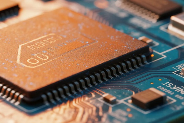
A AOI (Inspeção Ótica Automatizada) é um sistema de deteção industrial de alta precisão baseado na visão artificial, utilizado principalmente para o controlo de qualidade de placas de circuito impresso (PCBs). O seu princípio fundamental envolve a combinação de imagens ópticas de alta velocidade com algoritmos inteligentes para identificar automaticamente defeitos de montagem de PCB (por exemplo, desalinhamento de componentes, peças em falta) e problemas de soldadura (por exemplo, ponte, juntas frias).
Princípio de funcionamento do sistema AOI
1. Fase de aquisição de imagens
- Imagens de alta precisão: Utiliza câmaras CMOS/CCD industriais com iluminação anelar para captar as caraterísticas da superfície do PCB com uma resolução ao nível do mícron
- Captura multidimensional: Suporta inspeção 2D (juntas de solda/ecrãs) e análise de topografia 3D (altura da pasta de solda/coplanaridade dos componentes)
2.Pré-processamento de imagens
- Supressão de ruído: Aplica a filtragem Gaussiana e operações morfológicas para eliminar interferências ópticas
- Melhoria das funcionalidades: Utiliza a nitidez das margens e a fusão HDR para melhorar o contraste da área alvo
- Alinhamento de coordenadas: Efectua o registo CAD-para-imagem utilizando marcas fiduciais como pontos de referência
3.Deteção inteligente de defeitos
- Verificação baseada em normas: Verifica a colocação dos componentes/polaridade/morfologia da junta de soldadura de acordo com os critérios IPC-A-610
- Algoritmos híbridos:
Tradicional: Correspondência de modelos, análise de blob
Com recurso a IA:Redes CNN para a deteção de marcas de túmulos, solda fria, etc.
4.Sinalização de saída; Feedback
- Alerta por níveis: Acciona alarmes visuais/sonoros por gravidade do defeito (Crítico/Maior/Menor)
- Integração do sistema: Sincroniza os resultados NG para o MES com as coordenadas da estação de reparação
- Otimização do processo: Fornece dados SPC para a afinação de fornos de refusão/máquinas Pick-and-place
Vantagem da tecnologia AOI
1. Limitações da inspeção manual
As primeiras inspecções de PCB baseavam-se em verificações visuais manuais.No entanto, com o aumento da interligação de alta densidade (IDH) desenhos e produção em massa Os métodos manuais enfrentam três desafios críticos:
- Baixa fiabilidade: Propensos à fadiga e ao julgamento subjetivo, com taxas de fuga de defeitos superiores a 15%
- Ineficiência: Velocidade de inspeção <0,5 placas/minutoincompatível com os modernos ciclos de linha SMT
- Aumento dos custos: A mão de obra é responsável por 8%-12% dos custos totais de PCB, com longos requisitos de formação
2.Principais capacidades de deteção da AOI
Identifica com exatidão 7 grandes categorias de defeitos:
| Tipo de defeito | Exemplos | Precisão da deteção |
|---|---|---|
| Colocação de componentes | Falta, desalinhamento e polaridade invertida | ±25μm |
| Qualidade da junta de solda | Solda fria, ponte e solda insuficiente | 5% de tolerância de diâmetro |
| Defeitos na forma de chumbo | Condutas dobradas, levantadas e não coplanares | Resolução de 15μm |
Vantagens exclusivas em relação aos métodos tradicionais:
- Elimina os ângulos mortos dos testes: Detecta BGA underfill, componentes 0201 e outras áreas inacessíveis às sondas ICT
- Análise de dados em circuito fechado: A classificação de defeitos em tempo real (por exemplo, identificação de 30% de defeitos de impressão em stencil) permite a otimização do processo
3.Vantagens de desempenho quantificadas
| Métrica | Inspeção AOI | Inspeção manual | Melhoria |
|---|---|---|---|
| Precisão | Detecta Defeitos de 0,01 mm² | Limite humano: 0,1 mm² | 10 vezes melhor |
| Velocidade | 20 pranchas/minuto (via dupla) | 0,3 placas/minuto | 66x mais rápido |
| Consistência | CpK ≥1,67 | CpK ≤1.0 | Rendimento ↑40% |
4.Integração do fabrico inteligente
- Feedback em tempo real: Acciona os alertas MES com as coordenadas da estação de reparação (<Resposta em 2 segundos)
- Manutenção preventiva: A análise de tendências baseada em SPC prevê problemas como o entupimento do stencil
- Eficiência de custosTípico ROI <6 meses com 50-70% de redução de sucata
O papel crítico da AOI nas linhas de produção SMT
I. Quatro nós de inspeção principais da AOI no processo SMT
- Inspeção Pós-Pasta de Soldadura (Integração SPI-AOI)
- Função principal: Mede a espessura da pasta (±5μm), a área de cobertura e os defeitos de ligação
- Valor preventivo:A deteção precoce de obstrução/desalinhamento do stencil evita defeitos de refluxo (melhoria de 60% na taxa de interceção de defeitos)
- Colocação de componentes pós-chip (após o montador de chips)
- Foco: Componentes 0201/0402 em falta, invertidos ou desalinhados (precisão de ±15μm)
- Vantagem em termos de custos:O custo do retrabalho nesta fase é apenas 1/20 da correção pós-refluxo
- Colocação de componentes pós-CI (dispositivos de passo fino)
- Capacidade crítica: Identifica erros de polaridade QFP/BGA e coplanaridade de chumbo (resolução angular de 0,5°)
- Controlo do processo:Troca de dados em tempo real com máquinas pick-and-place para compensação automática de desvio
- Inspeção final pós-refluxo (rastreio exaustivo de defeitos)
- Principais desafios:
Deteção da morfologia da junta de soldadura em 3D (requer uma resolução de 10μm no eixo Z)
Inspeção de áreas sombreadas (por exemplo, terminações inferiores QFN) - Estatuto da indústria: Taxa de deteção de 92% vs. 99,5% para AOI pré-refluxo
II.Comparação técnico-económica: AOI pré-refluxo vs. AOI pós-refluxo
| Dimensão | AOI de pré-refluxo | AOI de pós-refluxo |
|---|---|---|
| Foco | Prevenção de processos | Garantia de qualidade |
| Métrica chave | Taxa de chamadas falsas <0,1% | Taxa de fuga ~8% |
| Eficiência de custos | $0.002/placa | $0,15/retrabalho de placa |
| Desafio técnico | Inspeção dinâmica a alta velocidade (≥45cm/s) | Reconstrução complexa de juntas de soldadura em 3D |
III.Recomendações de boas práticas
- Estratégia de seleção de equipamento
- Pré-refluxo: Dar prioridade à AOI de alta velocidade com tecnologia "on-the-fly" (por exemplo, Koh Young KY8030)
- Pós-refluxo:Deve incorporar microscopia confocal 3D (por exemplo, Omron VT-S730)
- Aplicação de dados em circuito fechado
- Estabelecer gráficos de controlo SPC (ativar automaticamente a limpeza do estêncil quando os defeitos da pasta são superiores a 3%)
- Alimentar os dados de desvio de colocação de volta para as máquinas de recolha e colocação através do MES (precisão de compensação de ±7μm)
- Tendências de evolução futura
- AOI virtual utilizando aprendizagem profunda (previsão do risco de defeitos na fase EDA)
- Inspeção multimodal (fusão de dados de raios X + AOI para modelação holística de juntas de soldadura)
Guia de referência rápida para inspeção AOI
1. Julgamento errado do carácter
- Questão: Chamadas falsas devido a marcações de componentes pouco nítidas/inconsistentes
- Soluções:
- Utilização imagiologia multi-espetral (visível + IV)
- Ajustar a tolerância da escala de cinzentos (ΔE < 15)
- Reduzir os controlos críticos de carácter
2.Pontos cegos da inspeção
- Pontos cegos comuns:
- Sombras de componentes altos → Anel luminoso de 45° + iluminação lateral
- Juntas de solda inferior BGA → Microscopia confocal de varrimento de camadas
- Componentes <3mm da borda da placa → Conceção de uma zona de proteção de 5 mm
3.Debate sobre as normas relativas às juntas de soldadura
- Parâmetros-chave:
- Componentes do chip: Ângulo de molhagem 25°-55°, Xc/Xi=1,2-1,8
- Componentes QFP: Filete de solda ≥50% de espessura de chumbo
- Regra de conceção:
  Extensão da almofada = Comprimento do componente × 0,25
 Espaçamento mínimo = Altura média do componente + 0,5 mm
4.Resultados da implementação
- Melhorias típicas:
Taxa de chamadas falsas ↓70%
Velocidade de inspeção ↑25% - Reparação de emergência:
Se o número excessivo de falsas chamadas → Desativar a verificação de caracteres ou ativar Modo de aprendizagem”
5.Tabela de resolução rápida de problemas
| Tipo de problema | Correção primária | Solução de cópia de segurança |
|---|---|---|
| Erros de carácter | Ajustar o limiar da escala de cinzentos | Desativar a verificação de caracteres |
| Falhas na junta de soldadura | Adicionar iluminação lateral | Zona de nova verificação manual |
| Interferência da sombra | Rodar o PCB 90° | Marcar como zona de exclusão |
Aplicações da tecnologia AOI e cobertura da indústria
1. Principais domínios de aplicação
- Fabrico de eletrónica SMT (Domínio primário)
- Objectivos de inspeção:
Qualidade da junta de soldadura (vazios/pontes/insuficiência de solda)
Colocação de componentes (desalinhamento/inversão/ausência)
Verificação da polaridade (orientação dos condensadores de tântalo/diodos) - Normas do sector:
IPC-A-610 Classe 3 (Classe aeroespacial/médica)
Precisão da deteção: ±15μm (nível do componente 0201)
- Produção de painéis de visualização (LCD/OLED)
- Inspecções críticas:
Defeitos de pixéis (pontos claros/escuros/defeitos de linha)
Precisão do alinhamento (desvio do painel <3μm)
Uniformidade do adesivo (tolerância de largura da cola UV ±50μm)
2.Aplicações industriais alargadas
| Setor | Casos de utilização típicos | Caraterísticas técnicas |
|---|---|---|
| Embalagem de semicondutores | Inspeção da altura dos ressaltos da bolacha (±1μm) | Microscopia confocal 3D |
| Eletrónica automóvel | Inspeção a 100% da junta de soldadura da ECU do motor (requisito de zero defeitos) | Sistema em linha à prova de vibrações |
| Biomédico | Verificação da integridade do canal do chip microfluídico | Interferometria de luz branca sub-micrónica |
3.Integração de tecnologias emergentes
- Implementação de Fábrica Inteligente
- A integração do sistema MES permite:
Monitorização do rendimento em tempo real (taxa de atualização de dados ≤2s)
Limiares de deteção adaptáveis (ajuste de parâmetros orientado por IA)
- Expansão inter-industrial
- Embalagem de alimentos: Controlo da integridade do selo da folha de alumínio (precisão de 0,1 mm)
- Indústria têxtil: Seleção automática de defeitos de tecido (velocidade de 30m/min)
4.Guia de seleção de tecnologias
- Prioridade ao fabrico de eletrónica:
- Sistemas integrados SPI+AOI 3D (por exemplo, Koh Young KY8030)
- Componente mínimo detetável: 01005 (40μm×20μm)
- Recomendações industriais gerais:
- Os sistemas AOI universais devem incluir:
Iluminação multi-espetral (para substratos de metal/plástico)
Índice de proteção IP54 (resistência ao pó/óleo)
Conclusão
A tecnologia de inspeção ótica automatizada (AOI), como um meio de controlo de qualidade central no fabrico moderno, expandiu-se do fabrico tradicional de eletrónica SMT para diversos campos, como painéis LCD, embalagens de semicondutores, eletrónica automóvel e biomédica. O seu valor central reside na combinação de imagens ópticas de alta precisão (± 15μm) e algoritmos inteligentes (por exemplo, aprendizagem profunda) para realizar a deteção automática de defeitos de juntas de solda, erros de colocação de componentes e problemas de polaridade e, ao mesmo tempo, ligação com o sistema MES para formar um circuito fechado de dados para promover a atualização da fabricação inteligente. No futuro, a AOI será profundamente integrada à manutenção preditiva de raios X e IA para romper ainda mais o limite de deteção e se tornar um "guardião da qualidade" indispensável na era da Indústria 4.0.


Publicações relacionadas