Tillverkningsfel i kretskort är sällan slumpmässiga.
De flesta defekter härrör från designbeslut, materialbegränsningar eller processinstabilitet, långt innan slutbesiktning sker.
Vid en besiktning kan många synliga problem upptäckas, förebyggande av defekter måste ske tidigare i tillverkningsprocessen.
Den här artikeln förklarar de vanligaste tillverkningsfelen för mönsterkort, deras grundorsaker och praktiska förebyggande strategier ur ett tillverkningsperspektiv.
För grundläggande kvalitetsfrågor, se: Vad avgör PCB-kvaliteten?
Innehållsförteckning
Vad betraktas som ett tillverkningsfel i mönsterkortstillverkningen?
Ett tillverkningsfel i kretskort är en avvikelse som:
- Påverkar elektrisk prestanda
- Kompromissar med mekanisk integritet
- Minskar den långsiktiga tillförlitligheten
- Bryter mot IPC- eller kundspecifikationer
Defekterna kan vara synlig, latent, eller progressivoch uppträder först efter termisk eller mekanisk påfrestning.
Defekter i det inre lagret
Vanliga defekter i det inre lagret
- Öppna kretsar
- Kortslutningar
- Överetsning eller underetsning
- Felregistrering mellan lager
Grundläggande orsaker och fördelarKärnbaserad HDI
- Felaktigheter i avbildningen
- Variation i etsningsprocessen
- Dålig uppriktning av det inre lagret
Eftersom de inre skikten förseglas under lamineringen är defekter i detta skede oåterkallelig.
Processens bakgrund: Förklaring av innerskiktets tillverkning
Borrningsrelaterade defekter
Typiska fel vid borrning
- Off-center hål
- Grater och smuts
- Trasiga borrkronor
- Dålig kvalitet på hålväggen
Grundläggande orsaker och fördelarKärnbaserad HDI
- För stort bildförhållande för borren
- Slitna verktyg
- Felaktig matning och hastighet
- Olämplig borrmetod
Borrfel påverkar direkt kopparpläteringens kvalitet och tillförlitlighet.
Jämförelse av metoder:
PCB-borrning vs laserborrning
Pläteringsdefekter
Vanliga problem med plätering
- Tunn koppar i vias
- Tomrum eller luckor
- Grov eller nodulär koppar
- Dålig vidhäftning
Grundläggande orsaker och fördelarKärnbaserad HDI
- Felaktig ytbehandling
- Inkonsekvent strömtäthet
- Kemisk obalans
- Vior med högt aspektförhållande
Pläteringsdefekter är en viktig orsak till Intermittenta fel och problem med termisk cykling.
Processdetaljer: Kopparpläteringsprocessen vid tillverkning av mönsterkort
Etsningsdefekter
Typiska etsningsdefekter
- Överetsade spår
- Underetcherade kopparbroar
- Variation i linjebredd
- Trace halsringning
Grundläggande orsaker och fördelarKärnbaserad HDI
- Ojämn koppartjocklek
- Aggressiv kemi för etsningsmedel
- Dålig processkompensation
- Tätt avstånd mellan spåren
I takt med att spårgeometrin blir finare påverkar etsningsdefekter i allt högre grad utbyte och tillförlitlighet.
Avkastningsinriktad analys: Process för PCB-etsning och kontroll av avkastning
Laminering och delamineringsdefekter
Vanliga problem med laminering
- Delaminering
- Blåsbildning
- Hålrum i harts
- Skift av lager
Grundläggande orsaker och fördelarKärnbaserad HDI
- Felaktigt lamineringstryck eller temperatur
- Dåligt val av prepreg
- Fuktabsorption
- Obalanserade stack-ups
Dessa defekter blir ofta uppenbara under montering eller termisk cykling, snarare än under den första provningen.
Materiell relation: Kostnad för PCB-material och lager
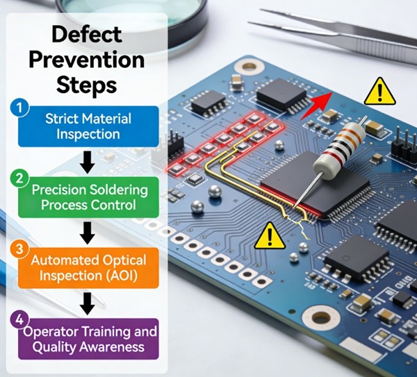
Lödmask- och ytfinishdefekter
Typiska defekter
- Felaktig inriktning av lödmask
- Dålig vidhäftning
- Pinholes
- Ojämn tjocklek på ytfinishen
Grundläggande orsaker och fördelarKärnbaserad HDI
- Otillräcklig ytbehandling
- Felaktiga härdningsförhållanden
- Kontaminering av processen
Dessa defekter kan leda till lödbryggor, korrosion och förkortad hållbarhetstid.
Undvikande av elektriska tester och dolda defekter
Det är inte alla defekter som upptäcks vid elektrisk provning.
Latenta defekter kan förekomma:
- Godkända inledande tester
- Går sönder efter termisk påfrestning
- Uppträder under fältarbete
Vanliga orsaker är bland annat:
- Marginell pläteringstjocklek
- Mikrosprickor i vias
- CAF-bildning
Designrelaterade defektrisker
Vissa defekter beror på designval snarare än tillverkningsfel.
Designfaktorer med hög risk inkluderar:
- Extremt fina spår och avstånd
- Vior med högt aspektförhållande
- Obalanserad distribution av koppar
- Alltför snäva toleranser
Koppling mellan design och kvalitet: Kostnadsfaktorer för PCB-design
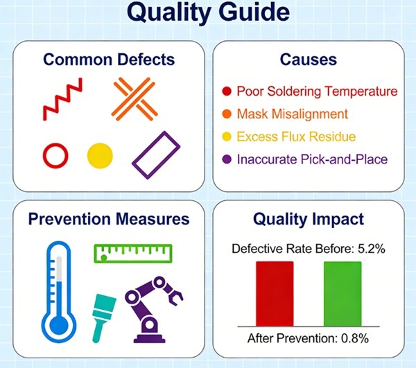
Hur man förebygger defekter vid tillverkning av mönsterkort
Effektivt förebyggande av defekter fokuserar på processtabilitetinte bara inspektion.
Viktiga förebyggande strategier inkluderar:
- Tidig DFM-granskning
- Konservativa konstruktionsmarginaler
- Kvalificerat materialval
- Övervakning av processens kapacitet
- Analys av avkastningsdata
På TOPFAST drivs arbetet med att förebygga defekter av uppströms processtyrning och databaserad återkopplingvilket minskar beroendet av screening i slutet av linjen.
Förebyggande av defekter vs tillverkningskostnad
Att förebygga defekter minskar ofta totalkostnaden.
Förmåner inkluderar:
- Högre avkastning
- Mindre omarbetning
- Färre förseningar
- Lägre risk för fel på fältet
Balans mellan kostnad och kvalitet: PCB:s tillverkningskostnad förklarad
Slutsats
Fel i mönsterkortstillverkningen är sällan isolerade händelser.
De är resultatet av samspelet mellan design, material och processtyrning.
Genom att förstå vanliga typer av defekter och deras grundorsaker kan ingenjörer och inköpare vidta proaktiva åtgärder för att förebygga defekter och förbättra den långsiktiga tillförlitligheten.
Denna artikel utgör en av grundpelarna i Kvalitet och tillförlitlighet för kretskort kluster.
FRÅGOR OCH SVAR: Defekter vid tillverkning av mönsterkort
A: Etsningsrelaterade defekter och pläteringsproblem är bland de vanligaste.
S: Nej. Inspektion upptäcker defekter men förhindrar inte deras grundorsaker.
A: Termisk stress under montering kan avslöja latenta defekter som introducerats tidigare.
S: Nej. Många defekter beror på design eller materialval.
S: Genom DFM-granskning och konservativ design anpassad till processens kapacitet.