Baskılı devre kartları (PCB'ler) modern elektronik ürünlerin temelini oluşturur. Pek çok mühendis PCB tasarımına odaklanırken, daha azı PCB'nin ne olduğunu tam olarak anlar. bir PCB'nin gerçekte nasıl üretildiği.
PCB üretim sürecinin anlaşılması yardımcı olur:
- Üretilebilirlik için tasarımın iyileştirilmesi (DFM)
- Üretim maliyetini azaltın
- Kalite sorunlarından kaçının
- PCB üreticileriyle daha etkili iletişim kurun
Bu makale bir PCB üretim sürecinin açık, adım adım açıklanmasıtarafından kullanılan gerçek dünya üretim uygulamalarına dayanmaktadır. TOPFASTprototip ve seri üretimi destekleyen profesyonel bir PCB üreticisi.
İçindekiler
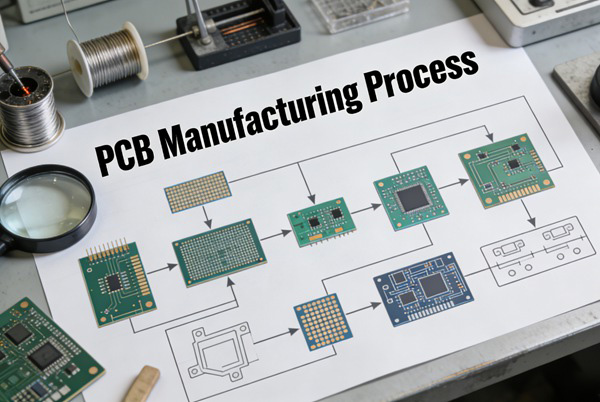
PCB Üretim Sürecine Genel Bakış
PCB karmaşıklığı değişebilse de, çoğu sert PCB aynı temel üretim akışını takip eder:
- İç katman imalatı
- Katman hizalama ve laminasyon
- Sondaj
- Bakır kaplama
- Dış katman görüntüleme ve aşındırma
- Lehim maskesi uygulaması
- Yüzey kaplaması
- Serigrafi baskı
- Elektrik testi ve son denetim
Her adım doğrudan şunları etkiler kalite, verim ve maliyet.
Adım 1 - İç Katman İmalatı
İç Katman Görüntüleme
Üretim bakır kaplı laminat levhalarla başlar. İstenen devre deseni, bir fotorezist ve UV maruziyeti kullanılarak bakır yüzeye aktarılır.
Anahtar faktörler:
- İz genişliği ve aralık doğruluğu
- Fotoğraf hizalama hassasiyeti
- Temiz oda ortamı
İç Katman Aşındırma
İstenmeyen bakır kimyasal olarak kazınarak uzaklaştırılır ve gerekli devre izleri bırakılır.
Üretim perspektifinden bakıldığında:
- Daha ince izler aşındırma zorluğunu artırır
- Fazla veya az aşındırma verimi etkiler
TOPFAST'ta, iç katman aşındırma parametreleri aşağıdakileri dengelemek için optimize edilir hassasiyet ve üretim istikrarı.
Adım 2 - Katman Hizalama ve Laminasyon
Çok katmanlı PCB'ler için, iç katmanlar prepreg ve dış bakır folyolarla istiflenir.
Laminasyon Süreci
- Isı ve basınç tüm katmanları birbirine bağlar
- Hassas hizalama, bağlantıların doğru şekilde yapılmasını sağlar
Maliyet ve kalite etkisi:
- Daha fazla katman laminasyon döngülerini artırır
- Sıralı laminasyon karmaşıklığı ve maliyeti artırır
Adım 3 - Delme
Delme, vialar ve bileşen uçları için delikler oluşturur.
Mekanik Sondaj
Şunun için kullanılır:
- Delikten geçen vialar
- Daha büyük delik boyutları
Sondaj maliyeti ile artar:
- Daha küçük delik çapları
- Daha yüksek en-boy oranları
- Yüksek sondaj sayıları
Lazer Delme (Gelişmiş PCB'ler)
Lazer delme için kullanılır:
- HDI PCB'lerde Mikrovialar
Bu işlem özel ekipman gerektirir ve üretim maliyetini artırır.
Adım 4 - Bakır Kaplama
Delme işleminden sonra delikler elektriksel olarak iletken olmalıdır.
Akımsız Bakır Biriktirme
Katmanlar arasında elektrik bağlantısı sağlamak için delinmiş deliklerin içine ince bir bakır tabaka bırakılır.
Elektrokaplama
İlave bakır kaplanmıştır:
- Yolları güçlendirin
- Gerekli bakır kalınlığını elde edin
Kaplama homojenliği, özellikle yüksek akımlı veya yüksek güvenilirlikli uygulamalar için güvenilirliği doğrudan etkiler.
Adım 5 - Dış Katman Görüntüleme ve Aşındırma
Dış katman devre deseni, iç katmanlara benzer bir işlem kullanılarak oluşturulur.
Temel zorluklar:
- Kaplamadan sonra iz doğruluğunun korunması
- Bakır kalınlığının kontrolü
- Kısa devre veya açılmaların önlenmesi
Dış katman işlemenin aşağıdakiler üzerinde büyük etkisi vardır nihai verim.
Adım 6 - Lehim Maskesi Uygulaması
Lehim Maskesinin Amacı
Lehim maskesi:
- Bakır izlerini korur
- Lehim köprülemesini önler
- Elektrik yalıtımını iyileştirir
Yaygın renkler arasında yeşil, siyah, mavi ve kırmızı bulunur. Yeşil, en uygun maliyetli ve yaygın olarak kullanılan seçenek olmaya devam etmektedir.
Lehim Maskesi Kalite Faktörleri
- Kayıt doğruluğu
- Maske kalınlığı
- Açılış tanımı
Kötü lehim maskesi kalitesi daha sonra montaj hatalarına neden olabilir.
Adım 7 - Yüzey İşlemi
Yüzey kaplaması açıkta kalan bakır pedleri korur ve lehimlenebilirlik sağlar.
Yaygın Yüzey Kaplama Seçenekleri
- HASL: Uygun maliyetli, yaygın olarak kullanılan
- ENIG: Düz yüzey, daha yüksek güvenilirlik
- OSP: Düşük maliyet, sınırlı raf ömrü
TOPFAST aşağıdakilere göre yüzey kaplamaları önerir varsayılan tercihler yerine uygulama gereksinimleri.
Adım 8 - Serigrafi Baskı
Serigrafi ekler:
- Bileşen referans belirleyicileri
- Polarite işaretleri
- Logolar veya tanımlayıcılar
Elektriksel olarak işlevsel olmasa da, şeffaf bir serigrafi montaj doğruluğunu ve bakımı iyileştirir.
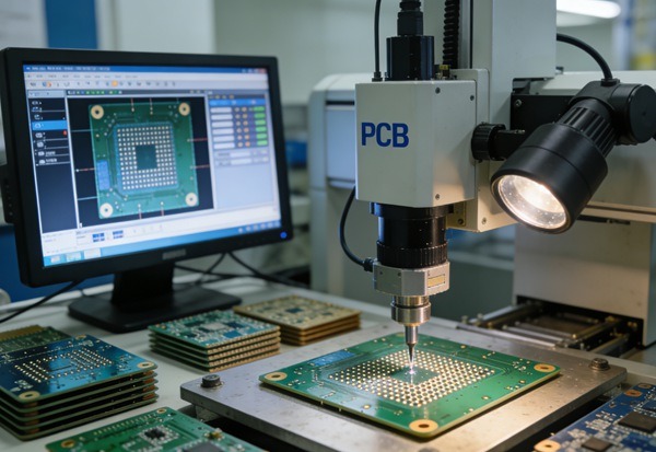
Adım 9 - Elektriksel Test ve Son Muayene
Elektriksel Testler
Elektrik testleri doğrular:
- Devamlılık
- İzolasyon
- Şort yokluğu ve açık
Bu adım, işlevsel güvenilirliğin sağlanması için gereklidir.
Nihai Kalite Denetimi
Son denetim şunları içerebilir:
- Görsel inceleme
- AOI (Otomatik Optik Muayene)
- Boyutsal kontroller
TOPFAST'ta denetim standartları aşağıdakilerle uyumludur IPC gereksinimleri ve müşteri spesifikasyonları.
PCB Üretim Süreci Maliyet ve Kaliteyi Nasıl Etkiler?
Her üretim adımı bir yenilik getiriyor:
- Süreç değişkenliği
- Verimle ilgili hususlar
- Maliyet etkileri
Yaygın maliyet etkenleri şunları içerir:
- Yüksek katman sayıları
- Küçük matkap boyutları
- Sıkı toleranslar
- Gelişmiş yüzey kaplamaları
Sürecin tamamını anlamak tasarımcıların şunları yapmasına olanak tanır PCB tasarımlarını hem maliyet hem de üretilebilirlik açısından optimize etme.
Üreticinin Bakış Açısı: TOPFAST PCB Üretimini Nasıl Optimize Ediyor?
Bir PCB üreticisi olarak TOPFAST şunlara odaklanır:
- Süreç standardizasyonu
- Erken DFM geri bildirimi
- Verim odaklı karar verme
- İstikrarlı ve ölçeklenebilir üretim
Gereksiz gelişmiş süreçleri zorlamak yerine, TOPFAST şunları vurgular tutarlı kalite sunan üretim dostu tasarımlar.
Sonuç
PCB üretim süreci, her biri nihai kartın performansına, güvenilirliğine ve maliyetine katkıda bulunan, dikkatle kontrol edilen bir dizi adımdır.
İç katman imalatından son denetime kadar PCB'lerin nasıl yapıldığını anlayarak mühendisler ve alıcılar daha iyi tasarım ve tedarik kararları verebilirler.
Üretim öncelikli bir yaklaşımla, TOPFAST, müşterilerin karmaşık tasarımları güvenilir, uygun maliyetli PCB'lere dönüştürmesine yardımcı olur.
PCB Adım Adım Üretim Süreci SSS
C: Standart PCB üretimi, karmaşıklığa ve miktara bağlı olarak tipik olarak 5-10 iş günü sürer.
C: Her adım önemlidir, ancak delme ve kaplama elektriksel güvenilirlik için kritik öneme sahiptir.
C: Evet. Çok katmanlı PCB'ler ek laminasyon ve hizalama adımları gerektirir.
C: Evet. Üretim kabiliyetleriyle uyumlu tasarımlar verimi artırır ve maliyeti düşürür.
C: TOPFAST, tutarlı kaliteyi sağlamak için standartlaştırılmış süreçler, DFM incelemesi ve kapsamlı denetim kullanır.