PCB failures are rarely random.
In most cases, failures are the result of design decisions, material choices, or manufacturing process limitations.
Understanding common PCB failure modes helps engineers:
- Identify root causes faster
- Improve design-for-manufacturability (DFM)
- Reduce field failures and warranty costs
This article provides a practical overview of the most common PCB failures, their symptoms, and how they are prevented in modern PCB manufacturing.
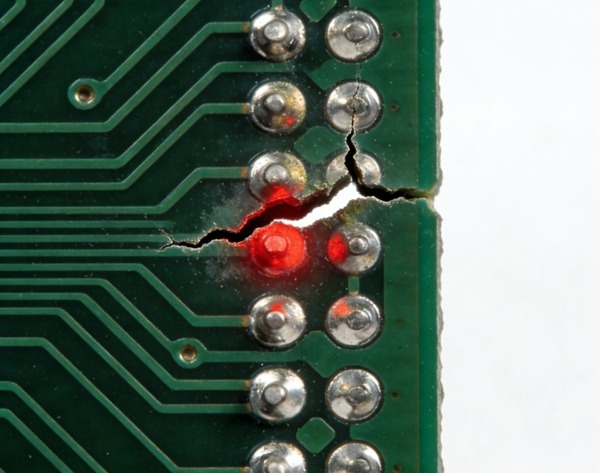
Table of Contents
What Is a PCB Failure?
A PCB failure occurs when a board no longer meets its electrical, mechanical, or reliability requirements.
Failures can appear:
- During electrical testing
- During PCB assembly
- After thermal cycling
- In real-world operation
Many failures originate long before the PCB is powered on.
Open Circuits and Short Circuits
Typical Symptoms
- Electrical test failure
- No signal continuity
- Unexpected current paths
Common Causes
- Incomplete copper plating
- Over-etching or under-etching
- Inner layer misregistration
Prevention Methods
- Controlled etching processes
- Electrical testing (E-test)
- AOI inspection during fabrication
Related: PCB Electrical Testing Explained
Delamination
Delamination refers to the separation between PCB layers or between copper and dielectric material.
Symptoms
- Blistering during soldering
- Internal voids visible by X-ray
- Reduced mechanical strength
Root Causes
- Excessive moisture absorption
- Improper lamination parameters
- Incompatible material selection
In-depth guide:
PCB Delamination Causes and Prevention
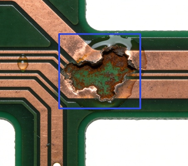
Conductive Anodic Filament (CAF) Failures
CAF is a latent failure mode that develops over time.
Characteristics
- Progressive insulation breakdown
- Often appears after months or years
- Triggered by moisture and voltage bias
Contributing Factors
- Glass fibre exposure
- Resin-rich areas
- High-humidity environments
Technical breakdown:
CAF Failure in PCB Explained
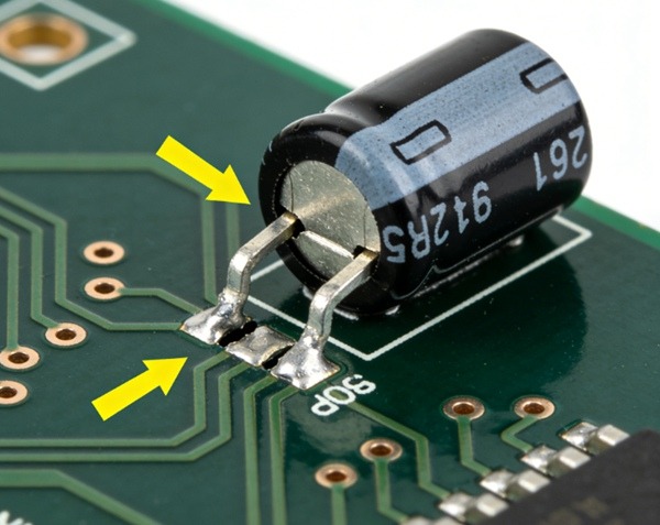
Solder Mask and Surface-Related Failures
Although often overlooked, surface-related defects can cause real functional problems.
Examples
- Solder mask cracking
- Poor adhesion
- Corrosion exposure
Prevention
- Proper surface preparation
- Controlled curing processes
- Material compatibility checks
How PCB Failure Analysis Is Performed
When failures occur, manufacturers use structured analysis methods.
Common tools include:
- Cross-section analysis
- X-ray inspection
- Thermal stress testing
- Electrical re-testing
Methods overview:
PCB Failure Analysis Methods Explained
Role of Manufacturing Process Control
Most PCB failures are preventable.
Key control areas include:
- Lamination profiles
- Copper plating thickness
- Material storage and handling
- Inspection and testing coverage
Manufacturers like TOPFAST integrate failure feedback into continuous process improvement rather than treating failures as isolated events.
Design Decisions That Increase Failure Risk
Design choices strongly influence failure probability.
High-risk design practices include:
- Extremely thin dielectrics
- Minimal annular rings
- High aspect ratio vias
- Tight spacing in humid environments
Design perspective:
PCB Quality and Reliability Design Guidelines
Conclusion
PCB failures are rarely caused by a single factor.
They are usually the result of interactions between design, materials, and manufacturing processes.
Understanding common failure modes allows engineers to:
- Design more robust PCBs
- Select appropriate materials
- Apply the right inspection and testing strategies
This article serves as the foundation of the PCB Failure Analysis content cluster.
Common PCB Failures FAQ
A: Most failures involve both.
A: No. Inspection reduces risk but cannot predict long-term degradation.
A: CAF and via cracks are often latent and require stress testing.
A: No. Process control matters more than cost alone.
A: When failures are intermittent, repeated, or field-related.