From Fundamentals to Advanced Strategies for AI and High-Speed Applications
The printed circuit board is the skeleton and nervous system of electronic products. The stability and performance of everything from simple microcontroller projects to complex AI servers are deeply rooted in the quality of the PCB design. This guide, compiled by the engineering expert team at TOPFAST, provides a complete roadmap from basic concepts to advanced strategies.
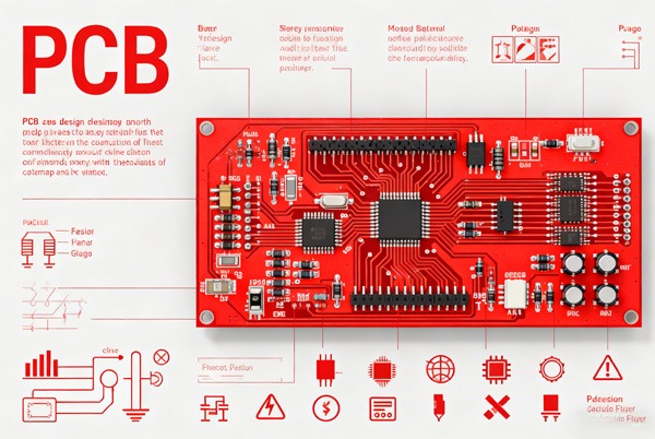
Table of Contents
Foundational PCB Design Process – A Robust Starting Point
For beginners, following a standardised design process is key to success.
1: Design Preparation – Schematic & Rule Definition
- Schematic Design: This is the logical foundation. Ensure symbols are correct, connections are accurate, and assign the proper footprint to each component.
- Pre-layout Planning: Early communication with your PCB manufacturer (like TOPFAST) is crucial. Obtain their Process Capability Document, defining parameters like minimum trace width/spacing, minimum hole size, stack-up structure, and set these as design rules to avoid DFM issues from the start.
2: Component Placement – The “Urban Planning” of an Electronic System
- Core Principle: “Location is everything.”
- Critical Components First: Place the main controller (CPU/FPGA), memory, and power management ICs first.
- Functional Modularisation: Group related circuits together (e.g., power supply, clock circuit, analogue section).
- Consider Thermal & Assembly: Distribute high-power components and plan thermal paths; place connectors and switches considering enclosure mechanics and user experience.
3: Routing – The Art and Science of Connection
- Power First: Route power and ground traces early, ensuring they are short and wide to minimise impedance.
- Critical Signals Priority: Route clocks, high-speed differential pairs, and sensitive analogue signals with the shortest, cleanest paths.
- 3W Rule: Maintain a parallel trace spacing of at least 3 times the trace width to reduce crosstalk.
- Grounding Strategy: Typically, use a split ground plane for digital and analogue sections, connected at a single point to avoid noise interference.
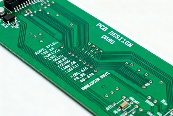
4: Post-Processing & Manufacturing File Generation
- DRC Check: Perform a final Design Rule Check to ensure no oversights.
- Generate Gerber & Drill Files: These are the standard files for manufacturing. Also, output an IPC-356 netlist for board flying probe testing to verify electrical connectivity matches the design.
- Communicate with the Fabricator: Provide a clear Assembly Drawing and Process Requirements (e.g., surface finish – Immersion Gold, HASL, or ENIG?). This enhances communication, ensuring a professional partner like TOPFAST accurately understands your needs for “Design for Manufacture.”
TOPFAST Tip: For initial prototypes, strongly recommend Electrical Test (E-test) and Flying Probe Test. This is the final, most cost-effective line of defense against potential shorts or opens.
Advanced Practices – Design Philosophy for AI and High-Speed Scenarios
When your design enters the GHz era for AI accelerator cards or high-speed switches, basic rules are merely the starting point. Success hinges on the co-design of integrity and manufacturability.
1. Paradigm Shift: From “Interconnect” to “System Co-Design”
A modern high-speed PCB is a 3D complex comprising signal transmission lines, a complex power distribution network (PDN), and a precise thermal management system. The goal shifts from “achieving functionality” to optimising the balance between Signal Integrity (SI), Power Integrity (PI), and Thermal Integrity.
2. The Critical Foundation: DFM and Reliability Design in Collaboration with TOPFAST
- Precise Impedance Control: It’s not just about trace width calculations. Confirm the specific core/prepreg materials with your manufacturer. TOPFAST’s engineering team offers stack-up advisory and impedance calculation services to ensure consistency from design to finished product.
- Advanced Via Design & Back-Drilling: Blind and Buried Vias are essential for high-density BGAs. For signals exceeding 10 Gbps, Back-Drilling (Stub Removal) is a standard process to eliminate stub effects and ensure signal integrity. Confirm capabilities for such advanced processes with TOPFAST during the design phase.
3. Simulation-Driven Design: “Prototyping” in the Virtual World
The old “design-fab-test-revise” cycle is costly and slow. The modern workflow should be an iterative “simulate-optimize-resimulate” process.
- SI/PI Co-Simulation: Analyse the impedance of the entire PDN. Optimise decoupling capacitor placement to ensure extremely low impedance at the chip’s power pins.
- 3D Electromagnetic (EM) Simulation: Use 3D full-wave solvers to accurately model the behaviour of complex connectors and vias over broad frequency ranges.
TOPFAST Case Study: In a client’s AI accelerator card project, the initial prototype showed high Bit Error Rate (BER) at 25 Gbps. Through combined channel simulation and TOPFAST’s PCB process analysis, it was identified that the dielectric loss (Df) of a specific laminate was higher than expected. Upon TOPFAST’s recommendation, the material was switched to M7NE, an ultra-low-loss material, and the glass weave style was optimized. This enabled stable operation at 32 Gbps with a BER better than 1E-12, without any design changes.
4. Designing for the Future: Partnering with Experts for Cutting-Edge Tech
The technology frontier is always advancing. Preparing for next-generation systems requires attention to:
- Ultra-Low Loss Materials: As data rates approach 112 Gbps PAM-4, standard FR-4 becomes untenable due to loss.
- System-Level Co-Design: Model and analyse the PCB, connectors, and cables as a single system.
- Deep Collaboration with a Partner like TOPFAST: From stack-up consultation and mid-cycle DFM review to implementing specialised processes (e.g., hybrid press-fit, rigid-flex), an experienced manufacturing partner provides not just products, but continuous engineering insight and assurance throughout the entire journey.
Conclusion
PCB design is a meticulous journey from logic to physics, from virtual to reality. Exceptional engineers are both scientists who master circuits and electromagnetic fields, and practitioners who deeply understand materials and processes. Partnering with a professional manufacturer like TOPFAST means having an engineering ally present throughout your journey—from design to mass production. This ensures your ideas, whether foundational or cutting-edge, are transformed into stable, reliable products with the highest quality and fastest speed, securing your competitive edge in the market.
PCB Design FAQ
A:Symptom: While impedance is calculated during design, the finished board fails to meet target values or exhibits discontinuities. This causes signal reflection, eye diagram closure, and system instability, especially in high-speed signals (e.g., HDMI, USB3.0, PCIe).
Root Cause:
The designed stack-up structure does not match the materials actually used by the fabricator (e.g., discrepancies in core/prepreg type or Dielectric Constant – Dk).
Trace width or dielectric thickness varies due to manufacturing tolerances.
Incomplete reference plane; signal traces cross over splits (anti-pads) in the plane.
Solution:
Engage with Your Fabricator (like TOPFAST) Early: Obtain and use the fabricator’s recommended stack-up table and impedance calculation parameters before layout.
Clear Annotation: Clearly mark which traces are controlled impedance, their target value, and reference layer on the Gerber files and fabrication notes.
Avoid Crossings: Ensure high-speed signal traces have a solid, continuous reference plane underneath.
A:Symptom: Significant voltage ripple at chip power pins, leading to random system errors, particularly during high-speed logic switching.
Root Cause:
Decoupling capacitors placed too far from the chip’s power pins, introducing excessive parasitic inductance, render them ineffective at high frequencies.
Use of inappropriate capacitor values or types (e.g., lacking small-value capacitors with good high-frequency characteristics).
The power path itself is too thin or long, exhibiting high impedance.
Solution:
“Proximity” Principle: Place small-value capacitors (e.g., 0.1µF, 0.01µF) as close as possible to the chip’s power pins, prioritising the shortest return path.
Optimise Vias: Use multiple vias for power/ground connections to reduce inductance.
Perform PDN Analysis: Validate the decoupling strategy using Power Integrity (PI) simulations, rather than relying solely on experience.
A:Symptom: Inability to route all signals from high-pin-count BGA chips (e.g., FPGAs, GPUs), or being forced to add many PCB layers just for fan-out, significantly increasing cost.
Root Cause:
Failure to utilise all available routing channels under the BGA. Reliance only on the traditional “dog-bone” pad fan-out.
Unfamiliarity with the fabricator’s microvia capabilities, leading to avoidance of blind/buried via technology.
Solution:
Use Via-in-Pad (VIP) Technology: Place laser-drilled microvias directly in the BGA pads. This is the preferred method for high-density BGA design.
Consult Manufacturing Capabilities: Confirm laser drilling precision and stacked via capabilities with TOPFAST. Plan for HDI (High-Density Interconnect) and blind/buried vias early in the design phase, which can often achieve higher routing density with fewer layers.
A:Symptom: High-power components (e.g., processors, power ICs) overheat under load, triggering thermal protection and causing performance throttling or system reset.
Root Cause:
PCB thermal design is neglected. Reliance is placed solely on the component’s heatsink without effectively conducting heat to the board or enclosure.
Insufficient copper area under the chip for effective heat spreading.
Lack of thermal vias, or they are insufficiently filled.
Solution:
Add Thermal Paths: Place a dense array of thermally filled vias in the PCB land pattern under the chip to rapidly transfer heat to the ground/power plane on the opposite side.
Increase Copper Area: Allocate larger copper areas on internal planes (especially ground) beneath heating components to aid heat dissipation.
Use Thicker Copper Foil: For high-current/high-heat areas, consult TOPFAST about using heavy copper foils (e.g., 2oz).
A:Symptom: The design functions perfectly in simulation/prototype, but small-batch production suffers from low yield, or issues like tombstoning, solder bridging, or cold joints occur during SMT assembly.
Root Cause:
Failure to adhere to basic Design for Manufacturability (DFM) and Design for Assembly (DFA) rules.
Poor component placement (e.g., placing fine-pitch QFPs on the wave-soldering side).
Improper stencil aperture design.
Solution:
Respect Process Capabilities: Ensure pad spacing and component clearance meet SMT equipment requirements. Avoid placing sensitive/tiny components in the shadow of larger parts during reflow or in wave-soldering areas.
Provide Accurate Centroid File: Generate a correct pick-and-place file (centroid file) containing reference designator, X/Y coordinates, and rotation, ensuring accurate machine programming.
Leverage the Fabricator’s DFM Check: Submit design files to TOPFAST for a professional DFM analysis before production. This can identify potential issues like poor pad design, acid traps, or insufficient assembly clearance early, avoiding costly re-spins.