Driven by green manufacturing and global environmental regulations, halogen-free PCBs are rapidly evolving from an optional feature to a standard component in high-end electronic products. This article provides a comprehensive industry insight by delving into the core standards, environmental advantages, complex manufacturing processes, and cost considerations of halogen-free PCBs, while also outlining their future development trajectory.
Table of Contents
What is a halogen-free PCB?
A halogen-free PCB refers to a printed circuit board in which the halogen content—specifically chlorine and bromine—in its substrate and solder mask, among other components, is strictly controlled in accordance with international environmental standards. According to the IEC 61249-2-21 and JPCA-ES-01-2003 standards, the limits for halogen content are as follows:
- Chlorine (Cl) and bromine (Br) content must each be ≤ 0.09% (900 ppm)
- Total halogen content (Cl + Br) must be ≤ 0.15% (1500 ppm)
These PCBs typically use halogen-free FR4 substrates, where traditional halogen-based flame retardants are replaced with more environmentally friendly alternatives such as phosphorus or nitrogen-based compounds. Halogen-free solder mask inks are also applied, making these boards suitable for applications with higher environmental and safety requirements.
Common halogen-free laminate materials available on the market include:
- Panasonic: R1566, R1566WN series
- Ventec: VT-447
- ITEQ: IT-170GRA1TC
- Isola: DE156 and GreenSpeed series
- Shengyi: S1550G, S1165 series
Environmental Advantages of Halogen-Free PCBs
Halogen-free PCBs (halogen-free printed circuit boards), as green materials in the modern electronics industry, demonstrate significant environmental benefits throughout their entire life cycle, particularly in terms of hazardous substance control, combustion safety, and long-term environmental friendliness.
1. Hazardous Substance Emission Control
- High Combustion Safety: Halogen-free PCBs do not release highly toxic gases such as dioxins (PCDD/Fs) during combustion, fundamentally avoiding the issue of toxic gas generation from traditional halogen-based flame retardants during incineration.
- Eco-Friendly Production Process: The use of halogen-containing chemical agents is reduced during production. Phosphorus or nitrogen-based flame-retardant resins (e.g., phosphate ester epoxy resin) are adopted, controlling halogen content from the source (individual halogen < 0.09%) and reducing wastewater and exhaust pollution.
- Long-Term Environmental Friendliness: Under harsh conditions such as humidity and high temperatures, halogen-free FR-4 materials do not suffer from the slow leaching of halogens, avoiding potential contamination of soil and water sources. Salt spray tests indicate that its corrosion resistance is approximately 50% higher than that of conventional FR-4.
2. Environmental Performance Comparison with Traditional PCBs
| Aspect | Halogen-Free PCB | Traditional Halogenated PCB |
|---|---|---|
| Combustion Byproducts | Carbon dioxide, water | Toxic gases like hydrogen bromide, dioxins |
| Smoke Toxicity | LC50 > 50mg/L (low toxicity) | LC50 ≈ 20mg/L (high toxicity) |
| Heavy Metal Content | < 10 ppm | Generally higher |
| Recycling Process | ~40% lower cost for harmless treatment | High cost and complex process |
| Long-Term Environmental Impact | No risk of pollutant leaching | Potential slow contamination |
Halogen-free PCBs meet the V0 flame retardancy standard in UL94 tests, and their toxic gas emissions comply with the strict limits of the EU RoHS 2.0 directive.
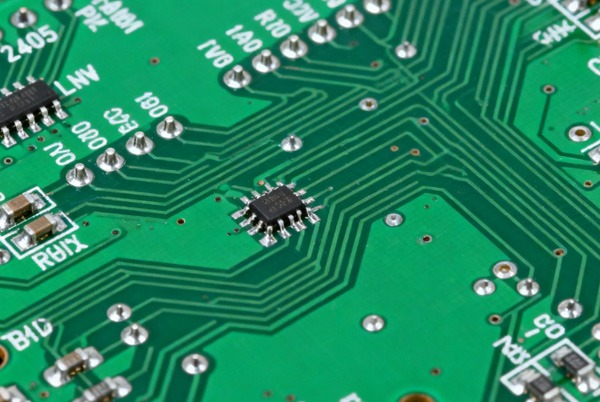
Halogen-Free PCB Manufacturing Processes
The manufacturing process of halogen-free PCBs is generally similar to that of traditional halogen-containing PCBs, but it imposes higher requirements in terms of material selection, process control, and environmental compliance. The key process steps are as follows:
1. Overview of the Process Flow
- Substrate Preparation: A flame-retardant system is constructed using phosphorus-containing epoxy resin, phenolic resin, and inorganic fillers (e.g., aluminum hydroxide) to replace traditional halogen-based flame retardants.
- Pattern Transfer: High-precision Laser Direct Imaging (LDI) technology is widely adopted to achieve micron-level fine circuits with line widths ≤ 50μm.
- Lamination and Drilling: For multi-layer boards, interlayer alignment deviation must be strictly controlled (typically within ±25μm), and laser drilling accuracy must reach ±5μm.
- Surface Treatment: Processes such as Electroless Nickel Immersion Gold (ENIG) or immersion silver are commonly used, requiring precise control of plating thickness and uniformity.
2. Process Differences Compared with Traditional Halogen-Containing PCBs
| Process Step | Halogen-Free PCB | Halogen-Containing PCB |
|---|---|---|
| Materials | Phosphorus/Nitrogen-based flame retardants (e.g., Al(OH)₃) | Brominated flame retardants (e.g., PBDEs) |
| Lamination Temperature | Higher (Td5% reaches 350–380°C) | Lower (Td5% around 320–340°C) |
| Environmental Requirements | Must comply with directives like RoHS; total halogen content < 1500 ppm | No strict restrictions; gradually being phased out |
How to Determine if a PCB is Halogen-Free
Accurately determining whether a PCB complies with halogen-free standards requires a comprehensive approach based on specific limit requirements, professional testing methods, and a formal certification process.
1. Core Criteria
A halogen-free PCB must meet the following halogen content limits, which serve as the fundamental basis for determination:
- Chlorine (Cl) Content ≤ 900 ppm
- Bromine (Br) Content ≤ 900 ppm
- Total Halogen (Cl + Br) Content ≤ 1500 ppm
Primary Reference Standards:
- IEC 61249-2-21
- JPCA-ES-01-2003
- IPC J-STD-709
2. Professional Testing Methods
| Method | Principle & Characteristics | Application Scenario |
|---|---|---|
| Ion Chromatography (IC) | High-precision quantitative analysis of chloride and bromide ions after sample combustion/extraction; considered the reference method. | Final determination, type testing |
| X-Ray Fluorescence (XRF) | Non-destructive, rapid screening for semi-quantitative analysis of chlorine and bromine. | Rapid preliminary inspection of incoming materials |
| Combustion-Ion Chromatography (C-IC) | Samples are combusted, and the products are analyzed via IC; particularly suitable for complex matrices. | High-precision detection of total halogen content |
3. Key Testing Equipment
- Ion Chromatograph: Core equipment for precise measurement of chloride and bromide ion content.
- X-Ray Fluorescence Spectrometer: Used for on-site rapid screening and preliminary judgment.
- Auxiliary Equipment: Automated Optical Inspector (AOI), Flying Probe Tester, etc., used for physical performance and reliability verification.
4. Certification and Quality Control Process
- Sample Preparation: Collect samples from batch products according to standard requirements.
- Laboratory Testing: Submit samples to an accredited third-party laboratory for analysis using standard methods.
- Reporting & Certification: Review the test report; obtain halogen-free certification upon compliance.
- Ongoing Control:
- Material Consistency: Ensure batch materials are consistent with submitted samples.
- Periodic Re-testing: Mandatory re-testing after material changes or process adjustments.
- Document Management: Properly archive all test reports and certificates.
Halogens in PCBs and the Structure of Halogen-Free PCBs
I. Definition and Common Forms of Halogens in PCBs
In the periodic table of chemical elements, halogens refer to the Group 17 (VIIA) elements, including fluorine (F), chlorine (Cl), bromine (Br), iodine (I), and the radioactive element astatine (At). In the electronics industry, the term typically refers to the first four non-radioactive elements.
In traditional PCB manufacturing, halogen compounds are commonly used as flame retardants:
- Historical Usage: Polybrominated biphenyls (PBB) and polybrominated diphenyl ethers (PBDE) were once widely used but are now explicitly banned in regions such as the European Union and China due to their toxicity.
- Current Situation: Other brominated flame retardants (e.g., tetrabromobisphenol A/TBBA or brominated epoxy resins) are still commonly used in standard FR-4 and CEM-3 laminates, meaning these PCBs are still classified as halogen-containing.
II. Health and Environmental Risks of Halogens in PCBs
Halogen-containing PCBs can release hazardous substances under specific conditions, posing significant risks:
- High Temperatures and Combustion Toxicity
- PBB and PBDE produce highly toxic dioxins, benzofurans, and black smoke when burned.
- Even currently permitted tetrabromobisphenol A (TBBA) may release hydrogen bromide (HBr) at temperatures exceeding 200°C and generate large amounts of toxic brominated smoke during combustion.
- Regulatory Status
- Although PBB and PBDE are banned, the use of other brominated flame retardants is not yet universally prohibited worldwide.
- This means that commonly available “standard FR-4” or “CEM-3” laminates, as long as they contain such non-prohibited flame retardants, do not qualify as halogen-free PCBs.
III. Structure and Material Properties of Halogen-Free PCBs
True halogen-free PCBs involve fundamental adjustments in material composition:
- Alternative Flame Retardant Systems: Phosphorus (P)- or nitrogen (N)-based compounds, or inorganic hydroxides (e.g., aluminum hydroxide), are used as flame retardants, eliminating bromine, chlorine, and other halogens at the source.
- Substrate Modification: Specially formulated halogen-free resin systems (e.g., halogen-free epoxy resins) are used as substrates to ensure the entire laminate meets halogen-free standards.
- Core Standards: The final product must comply with strict limits—chlorine (Cl) and bromine (Br) content each ≤ 900 ppm, and total halogen content ≤ 1500 ppm.
In summary, identifying whether a PCB is halogen-free depends on understanding its flame retardant system and substrate composition. Halogen-free PCBs, by utilizing alternative flame retardants and environmentally friendly substrates, maintain excellent flame resistance while avoiding the health and environmental risks associated with halogens. This makes them a solution aligned with the trend toward green electronic products.
Cost Comparison Analysis Between Halogen-Free PCBs and Traditional PCBs
1. Direct Production Cost Comparison
The production cost of halogen-free PCBs is typically 20%–30% higher than that of traditional PCBs, primarily due to differences in the following areas:
- Raw Material Costs
- Halogen-Free PCBs: Utilize phosphorus/nitrogen-based flame-retardant resins (e.g., phosphate ester epoxy resin), which result in substrate costs 30%–50% higher than those of traditional FR-4.
- Traditional PCBs utilize flame retardants, such as brominated epoxy resin (TBBPA), with standard FR-4 substrate costs ranging from ¥80 to ¥ 120 per square meter.
- Production Process Costs
- Halogen-Free PCBs: Require stricter temperature control and cleaner environments, increasing processing costs by 15%–20%.
- Traditional PCBs: Benefit from mature and stable production processes with high equipment utilization rates.
- Environmental Treatment Costs
- Halogen-Free PCBs: Higher standards for wastewater and exhaust treatment increase environmental costs by 10%–15%.
- Traditional PCBs: Lower environmental treatment costs but require handling of halogen-containing pollutants.
2. Unit Price Comparison
| PCB Type | Price Range (¥/m²) | Typical Application Scenarios |
|---|---|---|
| Halogen-Free PCB | 150–300 | High-end consumer electronics, automotive electronics, and medical devices |
| Traditional PCB | 100–200 | Household appliances, industrial controls, basic electronic products |
Specific Price Differences:
- Standard FR-4 Double-Layer Traditional PCB: ¥100–200 per square meter
- Halogen-Free FR-4 Double-Layer PCB: ¥150–300 per square meter (approximately 50% higher)
- High-End Halogen-Free Multilayer Boards (e.g., 6-layer): 1.5–2 times the cost of traditional counterparts
3. Long-Term Total Cost of Ownership Analysis
From a lifecycle perspective, halogen-free PCBs offer the following cost advantages:
- Maintenance Costs
- Halogen-Free PCBs: 50% better corrosion resistance, leading to lower maintenance costs.
- Traditional PCBs: Potential leaching of halogen pollutants may increase maintenance costs.
- Recycling and Disposal Costs
- Halogen-Free PCBs: 40% lower harmless treatment costs.
- Traditional PCBs: Higher costs and complexity in handling halogen-containing waste.
- Performance Degradation
- Halogen-Free PCBs: Stable performance in harsh environments, longer service life.
- Traditional PCBs: Possible performance degradation over time, requiring earlier replacement.
4. Key Factors Influencing Cost Differences
- Production Scale
- Small Batch (≤100 units): Price difference of 50%–80%
- Large Batch (≥1000 units): Price difference narrows to 20%–30%
- Process Complexity
- Simple Single-Layer Boards: ~30% price difference
- Complex Multilayer HDI Boards: ≥50% price difference
- Regional Variations
- Lower prices in industrial clusters (e.g., Southern China)
- Costs may be 10%–20% higher in other regions due to logistics
5. Industry Application Recommendations
Prioritize Halogen-Free PCBs for:
- Export products (must comply with RoHS and other regulations)
- High-demand sectors like medical devices and new energy vehicles
- Industrial equipment used in harsh environments
Consider Traditional PCBs for:
- Cost-sensitive consumer electronics
- Short-term use or frequently updated devices
- Products for domestic markets with lower environmental requirements
While halogen-free PCBs have higher initial costs, the price gap narrows with larger production scales, and their long-term total cost of ownership offers significant advantages. Companies should make decisions based on product positioning, market requirements, and lifecycle cost considerations.
Detailed Explanation of Common Certification Standards for Halogen-Free PCBs
As a core component of environmentally friendly electronic products, halogen-free PCBs are governed by a certification system that encompasses international specifications, industry technical standards, and regional regulations. The main certification standards are systematically outlined and explained below.
I. International Core Standards
- IEC 61249-2-21
A fundamental technical standard established by the International Electrotechnical Commission, which clearly specifies:
- Chlorine content ≤ 900 ppm
- Bromine content ≤ 900 ppm
- Total halogen content ≤ 1500 ppm
This standard applies to printed boards and interconnect structure materials and defines flammability test methods for reinforced substrates.
- JPCA-ES-01-2003
An industry standard issued by the Japan Printed Circuit Association, consistent with IEC requirements:
- Individual chlorine/bromine content < 0.09 wt%
- Total halogen content < 0.15 wt% (1500 ppm)
It is regarded as the baseline specification for defining halogen-free materials.
II. Industry Technical Standards
- IPC J-STD-709
A standard from the Association Connecting Electronics Industries that adopts IEC halogen limits and specifies:
- Definitions and classifications of halogen-free materials
- Applicability to PCB substrates and copper-clad laminates
It serves as an important technical reference in the electronics manufacturing supply chain.
- IPC-4101B
A substrate standard for high-performance applications, emphasizing:
- Compliance with halogen-free requirements while meeting flame retardancy ratings
- Suitability for high-reliability electronic products and harsh environments
III. Regional Regulatory Requirements
- EU RoHS Directive
Restrictions on hazardous substances in electrical and electronic equipment:
- Limits on heavy metals such as lead, mercury, and hexavalent chromium
- Polybrominated biphenyls (PBB) and polybrominated diphenyl ethers (PBDE) < 1000 ppm
This is a mandatory regulation for products entering the EU market.
- UL Certification (USA)
Focuses on product safety performance:
- Flame retardancy ratings
- Electrical safety characteristics
It is a key market access requirement for North America.
- EU REACH Regulation
Comprehensive control over the use of chemicals:
- Requires registration and evaluation of chemical substances used
- Restricts the use of Substances of Very High Concern (SVHC) in materials
Imposes stricter environmental requirements on PCB raw material selection.
IV. Key Points for Certification Implementation
- Testing Methods
- Ion Chromatography (IC): Precise determination of chlorine and bromine ions
- X-Ray Fluorescence (XRF): Rapid screening and preliminary assessment
- Combustion Ion Chromatography (C-IC): Accurate analysis of complex samples
- Certification Process
- Preparation of standard samples
- Testing by accredited laboratories
- Review of test reports
- Issuance of certification
- Quality Control
- Ensure batch materials are consistent with certified samples
- Conduct regular re-inspection and change management
- Maintain complete certification documentation for audits
The comprehensive halogen-free certification system reflects the electronics industry’s transition toward green manufacturing. Enterprises should establish a certification management mechanism covering the entire process from material selection to production, based on target market requirements, to ensure compliance with international environmental standards and enhance market competitiveness.
Analysis of Future Development Trends in Halogen-Free PCBs
Halogen-free PCBs, as key materials for green electronics manufacturing, are facing unprecedented development opportunities. The following analysis outlines their main development trends:
1. Continued Expansion of Market Scale
- The global PCB market is steadily growing, with an estimated size of $96.8 billion by 2025, of which China accounts for 52% of the global share.
- Halogen-free PCBs are in high demand in high-end sectors such as AI servers and new energy vehicles, with an expected annual compound growth rate exceeding 6%.
- The proportion of high-end products has significantly increased, with HDI boards and high-layer count boards growing at a rate of over 10%.
2. Continuous Technological Innovation
- Material Breakthroughs
Phosphorus/nitrogen-based flame-retardant resins are fully replacing traditional halogenated materials.
New substrate materials are emerging, with significantly improved dielectric properties. - Process Upgrades
Microvia technology: Laser drilling achieves 0.05mm microvias.
Fine line patterning: Semi-additive processes enable 0.02mm line widths.
Intelligent production: Increased adoption of automated equipment. - Performance Optimization
Significant improvement in thermal stability.
Effective reduction of the coefficient of thermal expansion.
3. Rapid Expansion into Application Fields
- 5G Communication: Base station construction drives a 25% increase in demand for high-frequency, high-speed PCBs.
- New Energy Vehicles: High-voltage systems make halogen-free FR-4 the material of choice.
- AI Servers: Surge in demand for high-layer count boards with 20+ layers.
- Medical Electronics: Safety requirements drive the adoption of halogen-free materials.
4. Increasingly Stringent Environmental Requirements
- Regulations such as the EU RoHS and REACH reinforce restrictions on halogens.
- China continues to advance pollution control in electronic information products.
- Full lifecycle green manufacturing has become an industry consensus.
5. Challenges and Opportunities Coexist
- Main Challenges
Production costs are 20-30% higher than traditional PCBs.
High technical barriers exist in areas such as high-frequency and high-speed applications. - Development Opportunities
Sustained growth in demand for environmentally friendly electronic devices.
Domestic companies are increasingly capturing market share in high-end sectors.
Emerging application areas provide a broad market space.
Professional Manufacturer of Halogen-Free PCBs
TOPFAST is a professional PCB solution provider with extensive expertise in the manufacture of halogen-free PCBs, specializing in rapid prototyping and small-batch production services. With our high-quality products and reliable on-time delivery, we have earned the trust and industry acclaim of global customers.
Our comprehensive product portfolio includes HDI boards, heavy copper boards, backplanes, semiconductor test boards, high-frequency and high-speed boards, as well as rigid-flex boards, catering to diverse needs across various sectors such as communications, medical devices, industrial control, automotive electronics, aerospace, and consumer electronics.
We are committed to superior quality, ensuring all our products comply with IPC standards and are certified under UL, RoHS, and the ISO9001 Quality Management System, providing customers with reliable and environmentally friendly solutions.
Adhering to our service philosophy of “high quality, fast delivery,” TOPFAST continuously strives to enhance customer satisfaction and aims to become the most trusted PCB partner for clients worldwide.
Conclusion
Halogen-free PCBs will continue to evolve toward high performance, environmental sustainability, and diversification. Technological innovation and application expansion will jointly drive industrial upgrading, providing crucial support for the green development of the electronics industry. As economies of scale materialize and technology matures, the cost advantage of halogen-free PCBs will become more pronounced, with market penetration expected to increase further.
Frequently Asked Questions (FAQ) About Halogen-Free PCBs
No. These are separate environmental standards, though they are often mentioned together:
Halogen-free: Limits chlorine (Cl) ≤ 900 ppm, bromine (Br) ≤ 900 ppm, and their sum ≤ 1500 ppm.
RoHS: Restricts lead, mercury, cadmium, hexavalent chromium, PBB, and PBDE to <0.1% (1000 ppm) each.
Although their scopes differ, many companies comply with both standards to meet market preferences.
Currently, halogen-free is not a global mandatory requirement, but it has become a significant environmental trend in the electronics industry. The driving forces include:
Demand from international brands and high-end markets
Ease of waste recycling and disposal
Emphasis on the environmental performance of products throughout their lifecycle
Standards such as IPC 4101B and JPCA-ES-01-2003 focus on chlorine and bromine because:
In the electronics industry, chlorine and bromine are the most commonly used halogen elements in flame retardants.
Other halogens like fluorine and iodine are rarely used as flame retardants in PCB manufacturing and have minimal environmental impact.
Compared to traditional PCBs, halogen-free PCBs typically offer:
Higher glass transition temperature (Tg)
Lower coefficient of thermal expansion (CTE)
Lower moisture absorption rate
Excellent heat resistance and long-term reliability
Yes. Many halogen-free substrates (e.g., Panasonic’s R1566 series, Isola’s GreenSpeed®) provide stable dielectric properties, making them suitable for high-frequency, high-speed designs and capable of meeting impedance control requirements.
Confirmation should be obtained through the following methods:
Request third-party test reports from suppliers (e.g., using the IEC 61249-2-21 standard)
Review their material certification documents (e.g., UL certification, RoHS compliance declarations)
Conduct regular sampling and send samples to accredited laboratories for precise testing, such as ion chromatography