In today’s world, from the smartphone in your hand to the medical devices that save lives, the core of electronic products is evolving in a common direction: smaller, lighter, more powerful, and more feature-rich. A key enabling technology behind this quiet revolution is the HDI PCB.
If you think of a PCB as merely a simple pathway connecting components, then HDI will fundamentally change your perception. It is not just a PCB with “denser lines”; it represents a profound transformation in design, materials, and manufacturing processes.
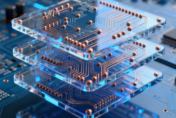
Table of Contents
HDI PCB: More Than Just “High Density”
HDI, or High-Density Interconnect, focuses on utilizing finer lines and smaller microvias to pack more functionality into a smaller space.
The essence of HDI technology lies in its advanced “microvia” process:
- Blind Vias, Buried Vias, and Via-in-Pad: Unlike through-holes that penetrate the entire board, HDI extensively uses blind vias (connecting only the surface layer to an inner layer) and buried vias (completely hidden inside the board, connecting inner layers). This liberates routing space on all layers and is key to achieving high density.
- Fewer Layers, Superior Performance: A well-designed 8-layer HDI board can offer performance and routing density far surpassing a traditional 12-layer through-hole board. This means lighter weight, more compact size, and better electrical signal integrity – the lifeblood of modern high-end electronic devices.
So, what is driving the demand for HDI?
- 5G and High-Speed Communication: 5G devices require extremely high signal transmission speeds and frequencies. The short paths and precise impedance control of HDI effectively reduce signal loss and interference.
- Portable and Wearable Devices: In smartwatches and AR/VR glasses, every cubic millimeter of space is crucial. HDI is the only way to achieve their “small form factor, powerful core.”
- Advanced Automotive Electronics & Aerospace: From ADAS systems to spacecraft control systems, these fields demand PCBs with extremely high reliability and density in extreme environments. HDI technology, combined with rigid-flex boards, meets complex spatial layout and vibration resistance requirements.
- High-End Medical Equipment: Devices such as endoscopes and pacemakers require powerful processing capabilities to be integrated into extremely compact spaces while ensuring absolute reliability. High-density interconnect (HDI) technology is the unparalleled solution for this challenge.
The Challenges of HDI Manufacturing: Why Choosing a Specialized Partner is Crucial
The exceptional performance of HDI comes with significant manufacturing complexities. A misstep in any single process can lead to the failure of an entire batch.
- Laser Drilling Precision: Creating microvias requires high-precision laser equipment. The position, size, and depth of the vias must be exact.
- Plating and Filling Technology: Achieving defect-free copper filling of microvias is a critical step, requiring precise chemical control and process expertise.
- Lamination Alignment: With 10 or more circuit layers, maintaining extremely high alignment accuracy during lamination is essential; otherwise, internal short circuits or open circuits can occur.
- Material Selection: High-frequency and high-speed applications require specific substrate materials, whose compatibility with HDI processes demands in-depth knowledge.
This is precisely where the value of a specialized manufacturer like TOPFAST comes in. We understand that HDI manufacturing is not merely a sequence of steps, but a precise science requiring profound experience, advanced equipment, and rigorous processes.
The TOPFAST Commitment: Your HDI Expert in the Heart of Chinese Manufacturing
Located in Zengcheng, Guangzhou, China – the heart of the Pearl River Delta, a world-class electronics manufacturing hub – TOPFAST is naturally endowed with superior supply chain and talent advantages. But we offer much more than just location.
1. Specialization in “Rapid Prototyping & Small Batch”: Your Innovation Accelerator
We deeply understand that during product R&D and start-up phases, you need not just a product, but speed and flexibility. TOPFAST specifically serves this need. When you upload your HDI design files, you will experience:
- In-Depth DFM Analysis: Our team of seasoned engineers (each with over 20 years of industry experience) conducts a thorough Design for Manufacturability analysis before production. We don’t just “build to print”; we are your design consultants, proactively offering optimization suggestions to enhance your board’s manufacturability and reliability from the source, making you more at ease.
- Seamless One-Stop Solution: From HDI Boards and Rigid-Flex Boards to High-Frequency & High-Speed Boards, our broad product capabilities mean you don’t need to find multiple suppliers for different board types. Whether it’s complex semiconductor test boards or durable heavy copper boards, we can handle them.
- Balancing High Quality and On-Time Delivery: We understand that “fast” does not mean “rushed.” By introducing advanced equipment, using premium materials, and strictly adhering to IPC standards and UL, RoHS, and ISO9001 certifications, we ensure that every PCB delivered to you meets our promised high-quality standards and reaches you on time, safeguarding your project timeline.
2. Our Capabilities, Serving Your Industries
TOPFAST’s HDI and specialty PCB products are actively used in cutting-edge fields like communications, medical equipment, industrial control, automotive electronics, and aerospace. We are proud to participate in these innovations that drive societal progress.
Conclusion
In this era of rapid electronics iteration, choosing the right PCB partner means laying the strongest possible foundation for your product. TOPFAST’s goal is not just to be your supplier, but to become your trusted partner.
We believe true partnership stems from deep understanding and professional support. The next time you face a complex design requiring HDI technology, TOPFAST is ready, with our expertise, reliability, and speed, to help turn your ideas into reality.
Frequently Asked Questions(FAQ)
A: No, it’s not just about density. The fundamental difference lies in the type of interconnection technology used. Standard PCBs primarily use “through-holes” that extend through the entire board, whereas the core of HDI PCBs involves the use of advanced structures, such as micro-blind vias and buried vias, to achieve shorter, more efficient connections within the multi-layer board. It’s like the difference between a regular road network and a multi-dimensional transport system with overpasses and underground tunnels – the latter significantly improves space utilization and signal transmission efficiency.
A: You should strongly consider HDI when your design faces one or more of the following challenges:
Space Limitations: The product requires miniaturization and lightweight design, such as wearable devices or micro-sensors.
Performance Bottlenecks: The need to handle high-speed, high-frequency signals (e.g., 5G, high-speed computing). HDI provides better signal integrity.
High Functional Integration: The need to fit more components into a limited space, e.g., high-end smartphones, compact medical instruments.
Reliability Requirements: For industries like automotive and aerospace that demand high reliability, the advanced structure and processes of HDI offer greater stability.
A: While the initial cost of HDI is indeed higher, it delivers core value that often far outweighs the cost through:
Reducing Total System Cost: A well-designed HDI board might achieve the same functionality with fewer layers, and potentially allow for the use of less expensive enclosures and connectors.
Enhancing Product Performance: Shorter signal paths mean faster speeds and lower power consumption, which translates directly into product competitiveness.
Accelerating Time-to-Market: Professional HDI manufacturers (like TOPFAST) provide upfront DFM analysis, identifying and resolving design issues early to avoid costly rework later, thereby speeding up your overall project timeline.
A: You should focus on the manufacturer’s capabilities in four key areas:
Technical Experience: Does the engineering team have experience handling complex stack-ups, laser drilling, and plating fill?
Equipment Precision: Do they possess advanced equipment like high-precision laser drilling machines and Automated Optical Inspection (AOI)?
Quality Systems: Do they strictly adhere to IPC standards and hold relevant certifications? This is the baseline for reliability.
Design Support Capability: Can they provide deep technical support and manufacturability analysis to help optimize your design? This is where real value is demonstrated.
A: This is crucial for customers in the R&D and innovation stages. The specific benefits include:
Faster Iteration Speed: Small-batch production is flexible, allowing quick responses to your design changes and accelerating your R&D verification cycles.
Higher Attention Level: Compared to factories chasing large-volume orders, we can allocate more engineering resources to your project and provide personalized technical support.
Lower Risk: You can access HDI manufacturing quality and technical support as professional as that for large-volume production, without the huge upfront investment, significantly reducing your initial risk and cost.