How important is shape when manufacturing PCB?
Table of Contents
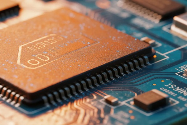
The Critical Role of PCB Shape Design
A PCB’s geometry is far more than cosmetic—it fundamentally influences:
- Mechanical Stability: Resistance to vibration and assembly stress
- Signal Integrity: High-frequency transmission quality
- Manufacturability: Compliance with fabrication limitations
- Cost Efficiency: Material utilization and panel optimization
1. Manufacturing Process Constraints
1.1 Panelization Cost Traps
Complex shapes (L-cut, irregular outlines) demand special handling:
- Nested panels require 2mm spacing buffers
- V-CUT blade lifespan decreases by 30% (non-linear paths)
- Skip-cut processes increase costs by 15-20%
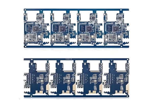
Case Study: A smartwatch’s L-shaped PCB initially achieved only 65% yield due to poor panel design. Switching to rectangular boards with strategic cutouts boosted yield to 92%.
1.2 Dimensional Tolerance Standards
| Application | Allowable Deviation | Inspection Method | Failure Risk |
|---|---|---|---|
| Smartphones | ≤0.1mm | Optical AOI | Solder voids |
| Automotive | ≤0.15mm | 3D Scanning | Vibration fractures |
| Medical Devices | ≤0.05mm | X-ray | Signal interference |
Consult a professional PCB designer
2. Signal Integrity Secrets
2.1 High-Frequency Routing Rules
- 90° Corners: Cause 8% impedance discontinuity at 1GHz (3dB return loss degradation)
- 45° Angles: Cost-effective for 1-10GHz (15% longer CAM processing)
- Curved Traces: Essential for 10GHz+, reduce EMI radiation by 40%
Test Data: A 5G base station PCB improved signal loss from 1.2dB/m to 0.7dB/m using curved traces.
2.2 Panelization Signal Hazards
- Never route differential pairs across panel gaps
- Maintain ≥1.2mm between clock lines and V-grooves
- Shielded borders can improve eye diagram opening by 15%
3. Mechanical Reinforcement Strategies
3.1 Edge Treatment Solutions
- Fillet Radius: 1-5mm (reduces stress concentration by 60%)
- Slot Design Standards:
- Isolation slots ≥1mm
- Thermal relief arrays ≥2mm spacing
- Stress-relief slots (0.1mm depth absorbs 30% deformation energy)
3.2 Material Selection Matrix
| Material Type | Flexural Strength | Cost Factor | Best Applications |
|---|---|---|---|
| Standard FR-4 | 345MPa | 1.0x | Consumer Electronics |
| High-Tg Materials | 400MPa | 1.3x | Automotive |
| Ceramic Substrates | 500MPa | 5.0x | Aerospace/Defense |
4. Design-for-Manufacturing (DFM) Checklist
4.1 Non-Negotiable Rules
- 5mm keep-out zone at edges (for components >25mm height)
- Minimum panel size 50×50mm (except metal-core PCBs)
- SMT processing range: 50×50mm to 350×250mm
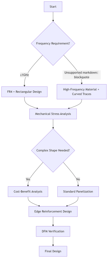
4.2 Engineer’s Decision Flowchart
Shape selection recommendations
- High-frequency (>10GHz) designs mandate curved traces + stripline structures
- Complex shapes may increase penalization costs by 20%—evaluate early
- Automotive PCBs prefer high-Tg materials with 3mm fillets
- Signal integrity prioritizes impedance continuity over absolute trace length


Related Posts