Inner layer fabrication is the first and most critical step in multilayer PCB manufacturing.
Once inner layers are laminated, any defect becomes permanent and extremely difficult—or impossible—to repair.
From a manufacturer’s perspective, the inner layer quality directly determines:
- Electrical performance
- Layer-to-layer alignment accuracy
- Overall yield
- Long-term reliability
This article explains how inner layers are fabricated, what can go wrong, and how manufacturers like TOPFAST control this process to ensure stable, high-quality PCB production.
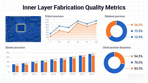
Table of Contents
What Is Inner Layer Fabrication?
Inner layer fabrication is the process of creating circuit patterns on the internal copper layers of a multilayer PCB before lamination.
Each inner layer contains:
- Signal traces
- Power planes
- Ground planes
Once fabricated, these layers are stacked and bonded together, forming the core electrical structure of the PCB.
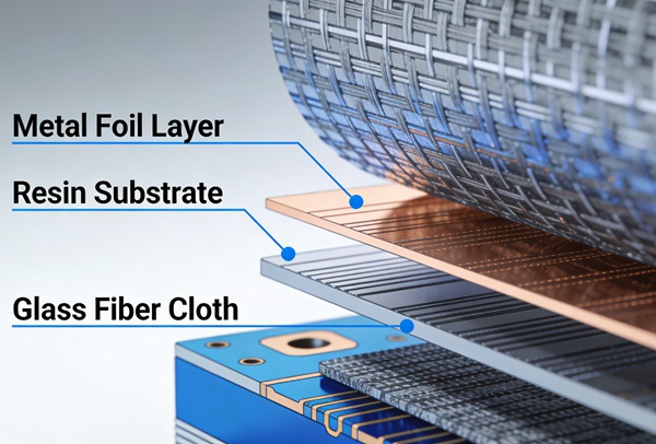
Materials Used in Inner Layer Fabrication
Copper-Clad Laminate
Inner layers start with copper-clad laminate consisting of:
- A fiberglass-reinforced epoxy substrate (commonly FR-4)
- Copper foil bonded to one or both sides
Copper thickness is typically:
- 0.5 oz
- 1 oz
- 2 oz (less common for inner signal layers)
Standard copper thickness improves process stability and cost control.
Step-by-Step Inner Layer Fabrication Process
Step 1 – Surface Preparation
Before imaging, the copper surface must be cleaned and treated to:
- Remove oxidation
- Improve photoresist adhesion
Poor surface preparation can cause:
- Trace definition defects
- Etching inconsistency
Step 2 – Photoresist Coating
A dry-film photoresist is laminated onto the copper surface.
Key considerations:
- Uniform thickness
- Proper lamination pressure
- Cleanroom conditions
This photoresist defines which areas of copper will remain after etching.
Step 3 – UV Exposure (Imaging)
The circuit pattern is transferred to the photoresist using:
- Phototools
- UV light exposure
Accuracy at this stage affects:
- Trace width and spacing
- Registration between layers
At TOPFAST, imaging accuracy is tightly controlled to support fine-line designs while maintaining yield.
Step 4 – Developing
After exposure, the board is developed to:
- Remove unexposed photoresist
- Reveal copper areas to be etched away
Incomplete development can cause:
- Residual photoresist
- Etching defects later
Step 5 – Etching
Chemical etching removes unwanted copper, leaving the desired circuit pattern.
Key challenges:
- Controlling etch rate
- Preventing undercutting
- Maintaining trace geometry
As the trace width decreases, etching becomes more difficult and yield-sensitive.
Step 6 – Photoresist Stripping
After etching, the remaining photoresist is stripped away, exposing the finished copper traces.
At this point, the inner layer circuit pattern is complete.
Common Inner Layer Defects and Their Impact
Over-Etching and Under-Etching
- Over-etching reduces trace width
- Under-etching leaves copper residue
Both can cause:
- Impedance deviation
- Shorts or open
Line Width Variation
Caused by:
- Imaging misalignment
- Etching instability
Line width variation affects:
- Signal integrity
- High-speed performance
Shorts and Opens
These defects are especially critical because:
- They may not be repairable after lamination
- They can cause total PCB failure
Inner Layer AOI (Automated Optical Inspection)
Why AOI Is Essential
Before lamination, inner layers are inspected using AOI to detect:
- Shorts
- Opens
- Missing copper
- Excess copper
This step prevents defective inner layers from entering the lamination.
Manufacturer’s Perspective
At TOPFAST, inner layer AOI is treated as a yield protection gate, not an optional step—especially for high-layer-count or fine-line PCBs.
How Inner Layer Quality Affects Final PCB Performance
Inner layer defects can lead to:
- Signal loss
- Crosstalk
- Power integrity issues
- Reduced reliability under thermal stress
For high-speed, high-density designs, inner layer accuracy is often more critical than outer layer appearance.
Design Factors That Influence Inner Layer Manufacturability
From a manufacturing perspective, cost and yield improve when designers:
- Avoid unnecessary ultra-fine traces
- Maintain consistent trace widths
- Use manufacturer-recommended stackups
- Balance copper distribution across layers
Early communication between design and manufacturing reduces inner-layer risk.
How TOPFAST Controls Inner Layer Fabrication Quality
TOPFAST applies a manufacturing-first approach to inner layer fabrication by:
- Using standardized imaging and etching parameters
- Applying AOI inspection before lamination
- Monitoring etch factor and line width variation
- Providing early DFM feedback on inner-layer designs
The goal is stable yield, predictable performance, and scalable production.
Cost Considerations in Inner Layer Fabrication
Inner layer cost increases with:
- Higher layer count
- Finer trace and spacing
- Tight impedance tolerances
- Advanced materials
Optimizing inner layer design is one of the most effective ways to reduce total PCB cost without sacrificing quality.
Conclusion
Inner layer fabrication forms the foundation of every multilayer PCB.
Once laminated, the inner layer quality cannot be corrected; it can only be accepted or rejected.
By understanding how inner layers are manufactured, designers and buyers can:
- Improve manufacturability
- Increase yield
- Reduce cost
- Enhance long-term reliability
With controlled processes and early DFM involvement, TOPFAST ensures the quality of the inner layer, supporting reliable and high-performance PCB manufacturing.
Related Reading: Step-by-step PCB Manufacturing Process
Inner Layer Fabrication Process FAQ
A: Inner layer fabrication is the process of creating circuit patterns on internal PCB layers before lamination.
A: Defects in inner layers cannot be repaired after lamination and directly affect reliability and performance.
A: Automated Optical Inspection (AOI) is used to detect shorts, opens, and pattern defects.
A: Yes. Finer traces require tighter process control and reduce yield, increasing cost.
A: TOPFAST uses standardized processes, AOI inspection, and DFM review to control inner layer quality.