PCB Classification
Classification and Applications of Printed Circuit Boards (PCBs)
Printed circuit boards (PCBs), as the core components of electronic devices, can be systematically classified based on different characteristics and application scenarios as follows:
Table of Contents
Classification by Conductive Layer Count
- Single-Sided PCB
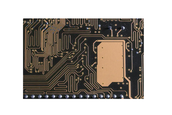
The most basic type of PCB, featuring a single copper layer with components mounted on one side and conductive traces on the other. It is simple in structure and low-cost, primarily used in early electronics and simple circuit designs. - Double-Sided PCB
Utilizes copper layers on both sides, with electrical connections between layers achieved through plated through-holes (PTHs). Compared to single-sided PCBs, they offer higher wiring density and design flexibility, making them the most widely used PCB type today. - Multilayer PCB
Consists of three or more conductive layers, bonded together with insulating dielectric materials and interconnected through vias. Multilayer PCBs enable complex circuit designs, meeting the high integration demands of modern electronics.
Classification by Substrate Material
- Rigid PCB
Manufactured using inflexible, sturdy base materials, including:
- FR-4 (fiberglass epoxy)
- Paper-based substrates
- Composite substrates
- Ceramic substrates
- Metal-core substrates
- Thermoplastic substrates
Widely used in computers, communication equipment, industrial controls, and more.
- Flexible PCB
Made with bendable insulating substrates, allowing for folding, rolling, and bending. Ideal for portable electronics such as smartphones and tablets. - Rigid-Flex PCB
Combines rigid and flexible sections, providing structural support while allowing bending, making them suitable for 3D assembly applications.
Specialized Functional PCBs
- Metal-Core PCB (MCPCB)
Composed of a metal base, insulating layer, and circuit layer, offering superior heat dissipation. Mainly used in high-heat applications like LED displays/lighting and automotive electronics. - Heavy Copper PCB (≥3 oz copper thickness)
Features:
- High current/voltage handling
- Excellent thermal performance
- Demanding manufacturing processes
Applications: Industrial power supplies, medical equipment, military electronics, etc.
- High-Frequency PCB
Characteristics:
- Low dielectric constant materials
- Strict signal integrity requirements
- High-precision fabrication
Applications: Communication base stations, satellite systems, radar, etc.
- High-Speed PCB
Features:
- Low-loss dielectric materials
- Precise impedance control
- Minimal insertion loss
Applications: Networking equipment, servers, data storage systems, etc.
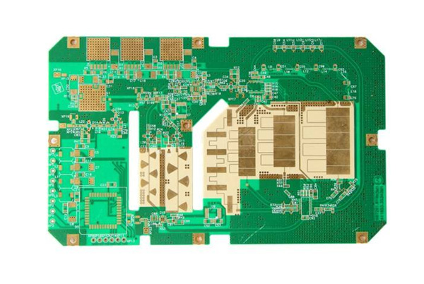
Advanced Multilayer PCB Technologies
- HDI (High-Density Interconnect) PCB
Technical Features:
- Microvia technology (laser drilling)
- Sequential lamination
- Ultra-high wiring density
Applications: Smartphones, automotive electronics, aerospace, etc.
- IC Substrate PCB
Functional Features:
- Direct chip mounting
- High pin-count design
- Miniaturized packaging
Applications: Memory chips, processors, sensors, and other semiconductor devices.
With advancements in electronics, PCBs continue to evolve toward higher layer counts, greater precision, and increased density. Emerging PCB technologies are driving innovation in electronic product development.


Related Posts