Optimizing cost and yield is essential for delivering reliable, affordable PCBs.PCB fabrication focuses on the bare board manufacturing stage, which forms the foundation of the complete PCB manufacturing workflow.
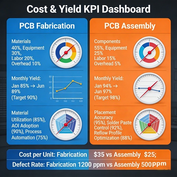
Both fabrication and assembly contribute significantly to overall production cost and potential yield loss.
By analyzing process impact, manufacturers like TOPFAST provide strategies to:
- Reduce scrap and rework
- Improve throughput
- Maintain consistent quality
For context on how fabrication and assembly differ, see: PCB Fabrication vs PCB Assembly
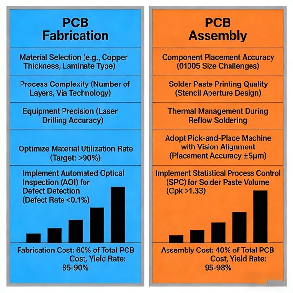
Table of Contents
Cost Drivers in PCB Fabrication
PCB fabrication cost depends on several factors:
- Layer count and complexity: More layers increase materials and processing steps.
- Copper weight and thickness: Heavy copper or uneven distribution raises plating and etching costs.
- Hole size and aspect ratio: Small or high-aspect-ratio vias increase drilling and plating difficulty.
- Board dimensions and panel utilization: Poor panelization increases material waste.
Understanding how these fabrication parameters affect reliability is important; see Inner Layer Fabrication Explained and Etching Process and Yield Control Explained.
Optimization Tip: Designers can reduce cost by standardizing layer counts, optimizing copper distribution, and reviewing drill specifications early in the DFM stage.
Cost Drivers in PCB Assembly
Assembly cost is influenced by:
- Component types and packaging: BGAs and fine-pitch components require more precise placement and inspection.
- Placement volume: Higher component density increases pick-and-place machine time.
- Soldering methods: Reflow vs wave soldering affect process time and yield.
- Testing and inspection requirements: AOI, X-ray, ICT, and functional tests add labor and equipment costs.
Fabrication quality directly affects assembly efficiency. Misaligned vias or poor plating can increase assembly rework; see PCB Drilling vs Laser Drilling and Copper Plating Process Explained
Yield Optimization Strategies in Fabrication
Early DFM Review
- Identify high-risk features: fine traces, dense vias, heavy copper zones.
- Adjust designs to match manufacturing capabilities, improving first-pass yield.
Process Control
- Monitor etching, plating, and drilling parameters.
- Use statistical process control (SPC) to detect deviations early.
Material and Vendor Selection
- Use consistent copper foil and laminate suppliers.
- Verify material compatibility with process requirements to avoid defects.
For a deeper dive into fabrication yield management, see Etching Process and Yield Control Explained
Yield Optimization Strategies in Assembly
Component Placement Accuracy
- Calibrate pick-and-place machines regularly.
- Use fiducials and alignment marks to ensure precise positioning.
Soldering Quality Control
- Optimize reflow profiles for thermal stress and solder wetting.
- Use wave soldering settings that prevent bridging and voids.
Inspection and Testing
- Combine AOI, X-ray inspection, and functional testing.
- Provide feedback loops to correct recurring defects early.
Assembly yield is directly impacted by fabrication quality; see Copper Plating Process Explained and PCB Drilling vs Laser Drilling.
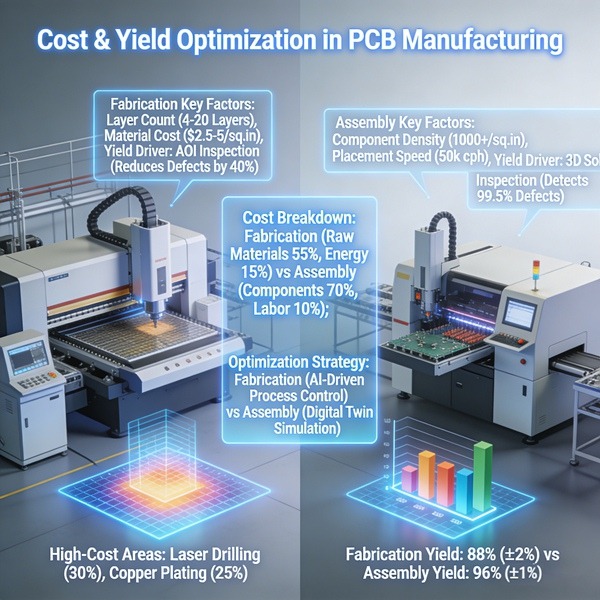
Balancing Cost and Yield
Effective PCB manufacturing balances minimizing cost with maximizing yield:
- Avoid over-specification that unnecessarily increases cost
- Do not compromise on critical features that reduce reliability
- Collaborate between design, fabrication, and assembly teams early in the product lifecycle
At TOPFAST, cost-yield optimization is approached as a system-level strategy, integrating insights from fabrication and assembly to achieve high-quality, cost-effective production.
Best Practices for Cost & Yield Optimization
- Standardize designs with manufacturable trace widths, spacing, and pad sizes
- Minimize high-aspect-ratio vias and unnecessary microvias
- Optimize panel layout to reduce material waste
- Align fabrication tolerances with assembly capabilities
- Use early inspection and in-process monitoring to catch deviations
Refer back to PCB Fabrication vs PCB Assembly for the full process overview.
Conclusion
Optimizing cost and yield requires holistic thinking across fabrication and assembly.
By carefully managing design, material, and process parameters, engineers can:
- Lower overall production costs
- Increase yield and reliability
- Reduce rework and scrap
Professional manufacturers like TOPFAST integrate these practices into daily operations to deliver reliable PCBs at competitive costs.
PCB Cost & Yield Optimization FAQ
A: Layer count, copper weight, hole size, and board dimensions significantly affect fabrication cost.
A: Component type, placement complexity, soldering method, and testing requirements determine assembly cost.
A: Early DFM review, strict process control, and consistent material selection improve fabrication yield.
A: Accurate placement, optimized soldering, and thorough inspection/testing improve assembly yield.
A: TOPFAST integrates fabrication and assembly insights, monitors processes, and applies DFM feedback to achieve high-quality, cost-effective PCBs.