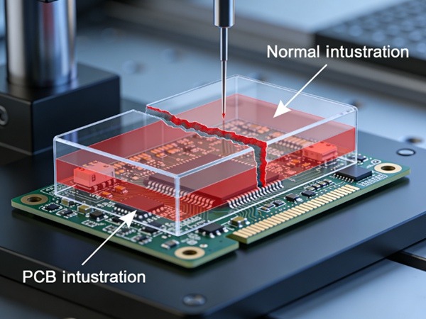
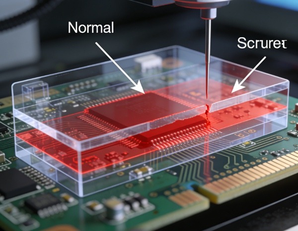
PCB delamination is one of the most destructive and often irreversible failure modes in printed circuit boards.
Unlike surface defects, delamination occurs inside the PCB structure, separating copper layers or dielectric materials and compromising mechanical strength, electrical insulation, and long-term reliability.
This article explains:
- What PCB delamination is
- Why it occurs
- How manufacturers detect and prevent it
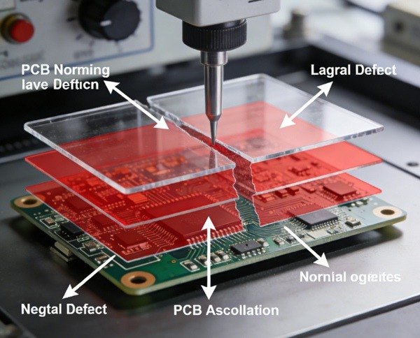
Table of Contents
What Is PCB Delamination?
PCB delamination refers to the loss of adhesion between layers within a PCB.
It may occur between:
- Copper foil and dielectric
- Adjacent dielectric layers
- Resin and glass fiber interfaces
Once delamination begins, it often propagates under thermal or mechanical stress.
Common Symptoms of PCB Delamination
Delamination may not always be visible at first.
Typical Symptoms
- Blistering or bubbling after soldering
- Internal voids detected by X-ray
- Sudden insulation resistance drop
- Mechanical weakness during assembly
Detection methods:
X-Ray Inspection in PCB Manufacturing
Primary Causes of PCB Delamination
H3: Excessive Moisture Absorption
Moisture trapped in PCB materials expands rapidly during soldering or reflow.
This expansion creates internal pressure that can separate layers.
Contributing factors include:
- Improper material storage
- High-humidity environments
- Long exposure before assembly
Incorrect Lamination Parameters
Lamination is a critical process in multilayer PCB fabrication.
Delamination may result from:
- Insufficient lamination pressure
- Inadequate resin flow
- Incorrect curing temperature or time
Process overview:
PCB Lamination Process Explained
Material Incompatibility
Not all PCB materials bond equally well.
Risk factors include:
- Mixing materials with different glass transition temperatures (Tg)
- Low peel strength copper foils
- Poor resin-to-glass adhesion
Material selection strongly influences delamination risk.
Thermal Stress and Repeated Heating
Repeated thermal cycles cause:
- Z-axis expansion stress
- Fatigue at copper-resin interfaces
High-layer-count boards are especially vulnerable.
Reliability link:
PCB Thermal Reliability Testing
Design Factors That Increase Delamination Risk
Design decisions often amplify delamination risk.
High-Risk Design Practices
- Very thin dielectric layers
- High copper density imbalance
- Large copper planes without relief
- Inadequate spacing near board edges
Early DFM review helps mitigate these risks.
How PCB Delamination Is Detected
Common Detection Methods
- X-ray inspection
- Cross-section analysis
- Thermal stress testing
- Visual inspection after soldering
Inspection hub:
PCB Inspection & Testing Explained
Preventing PCB Delamination
Controlled Material Storage
- Vacuum-sealed packaging
- Temperature and humidity monitoring
- Proper bake-out procedures
Optimised Lamination Control
- Verified pressure profiles
- Controlled resin flow
- Consistent curing cycles
Design-for-Reliability Practices
- Balanced copper distribution
- Adequate dielectric thickness
- Material compatibility verification
Relationship Between Delamination and Other PCB Failures
Delamination often triggers secondary failures:
- Via cracking
- CAF formation
- Insulation breakdown
Related failures:
Common PCB Failures Explained
Industry Perspective on Delamination Control
In modern PCB manufacturing, delamination prevention is addressed through:
- Material qualification
- Process window control
- Inspection feedback loops
Manufacturers like TOPFAST treat delamination as a system-level reliability issue, not just a single process defect.
Conclusion
PCB delamination is a complex failure mode influenced by materials, design, and manufacturing conditions.
While it cannot always be eliminated, it can be effectively controlled through:
- Proper material handling
- Optimised lamination processes
- Thoughtful design decisions
Understanding delamination mechanisms is essential for building reliable, long-lasting PCBs.
PCB Delamination FAQ
A: No. Once delamination occurs, the PCB is typically unusable.
A: It reduces risk but does not eliminate it.
A: Yes, especially under thermal cycling or high humidity.
A: Yes, due to higher internal stress.
A: Often only after stress or advanced inspection.