The distinction between PCB fabrication and PCB assembly is critical for engineers, designers, and procurement teams.
Understanding both processes helps in:
- Reducing manufacturing errors
- Optimising cost and lead time
- Planning for test and quality control
In this article, we will explore the main differences, challenges, and key considerations from TOPFAST’s professional PCB manufacturing perspective.
For a detailed overview of the overall PCB manufacturing process, see our hub page: PCB Manufacturing Process
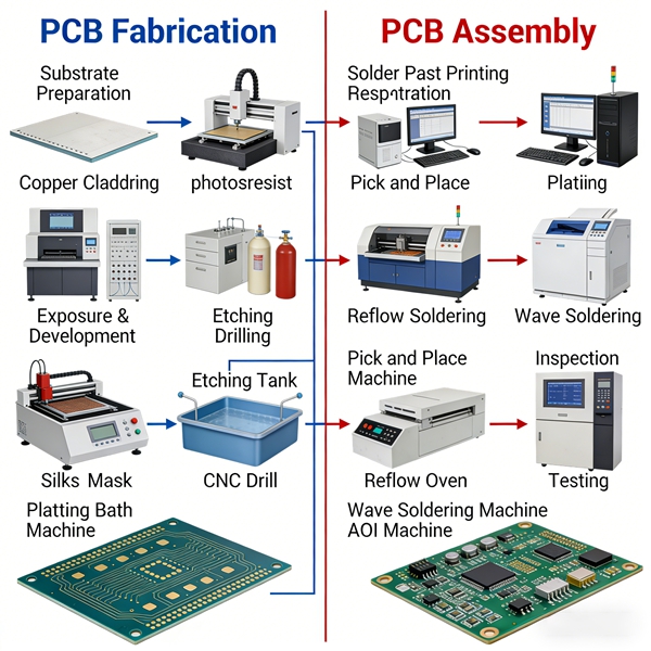
Table of Contents
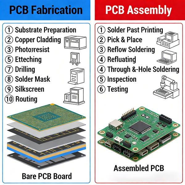
What is PCB Fabrication? (The Skeleton)
PCB Fabrication is the mechanical process of creating the bare circuit board. It involves:
- Material Selection: Choosing the right substrate to manage manufacturing costs.
- Lamination & Etching: Creating the conductive copper layers.
- Drilling: Utilising mechanical or laser drills for HDI PCB manufacturing.
- Surface Finish: Applying HASL or ENIG to protect copper and ensure solderability.
What is PCB Assembly? (The Nervous System)
PCB Assembly is the process of soldering SMD electronic components and through-hole parts onto the fabricated board.
- SMT Processing: Automated high-speed placement of tiny components.
- Reflow & Wave Soldering: Forming permanent electrical joints.
- Testing: Using methods to test capacitors and overall circuit logic.

Critical Differences at a Glance
| Feature | PCB Fabrication | PCB Assembly (PCBA) |
| Output | Bare board (No components) | Functional electronic device |
| Primary Goal | Physical architecture & connectivity | Electrical functionality & performance |
| Main Materials | Copper, FR-4, Solder Mask | SMD Components, Solder Paste |
| Key Check | DFM (Design for Manufacturing) | DFA (Design for Assembly) |
How to Smoothly Transition from Fabrication to Assembly
- Unified DFM/DFA Review
Ensure your PCB design decisions account for both the copper etching limits and the pick-and-place machine clearances.
- BOM Optimization
Provide a complete Bill of Materials (BOM) with exact manufacturer part numbers to avoid component mismatches.
- Coordinate the Stack-up
Match your PCB stack-up design with the thermal requirements of the reflow soldering oven.
- Panelization Strategy
Use panel sizes that maximise material usage in fabrication while remaining compatible with SMT conveyors.
- Quality Traceability
Implement serial numbers on the bare board during fabrication to track the PCBA processing history.
PCB Fabrication vs PCB Assembly FAQ
A: Absolutely. ENIG is preferred for fine-pitch SMD components, while HASL is a cost-effective choice for larger, less complex designs.
A: Misaligned layers, poor drilling, or plating issues can cause soldering defects, component misplacement, and thermal stress during assembly.
A: Yes, but using a turnkey provider like Topfast reduces communication errors and speeds up the overall manufacturing budget management.
A: Designing with proper spacing, pad sizes, and copper balance ensures manufacturability and reduces yield loss in both fabrication and assembly.
A: TOPFAST applies a manufacturing-first perspective, controlling process quality, yield, and reliability from fabrication to final assembly.
A: Incorrect footprint pads. If the fabrication pad is too small, the PCBA processing will result in poor solder joints or “tombstoning.”
A: We use AOI, X-ray, and functional testing. You can also manually test capacitors during the debugging phase of your prototype.
A: Generally, PCBA is more expensive due to the cost of SMD electronic components and the specialized precision equipment required.
Conclusion
Understanding the distinction between Fabrication and Assembly allows for better project planning and cost control. At Topfast, we bridge this gap by offering seamless, high-reliability PCB Assembly services.
Ready to move from design to functional hardware? Get a Unified PCB & PCBA Quote from Topfast today.