PCB failure analysis is a systematic process that identifies the reasons for a printed circuit board’s failure and determines the root cause.
Unlike inspection, which detects defects, failure analysis explains how and why defects formed—often after the PCB has already failed in the field or during reliability testing.
This article outlines the most common PCB failure analysis methods and when each should be used.
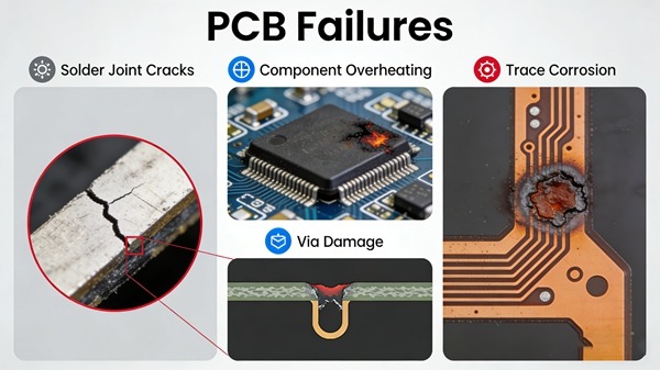
Table of Contents
Why PCB Failure Analysis Is Necessary
Failure analysis is essential when:
- Failures are intermittent
- Failures occur after environmental stress
- Multiple boards fail in similar ways
- Root cause is unclear after inspection
It provides critical feedback for improving design, materials, and manufacturing processes.
Failure overview:
Common PCB Failures Explained
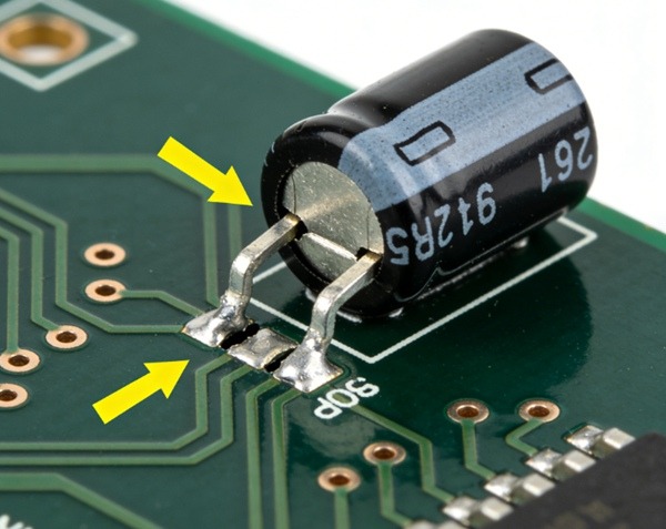
Electrical Failure Analysis
Electrical analysis is often the first diagnostic step.
Common Techniques
- Continuity testing
- Insulation resistance (IR) testing
- Leakage current measurement
Best Used For
- Opens and shorts
- Intermittent failures
- CAF-related leakage
CAF context:
CAF Failure in PCB Explained
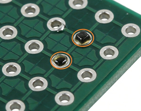
Cross-Section Analysis
Cross-sectioning physically exposes internal PCB structures.
What It Reveals
- Via barrel cracks
- Copper plating thickness
- Delamination and voids
- Resin starvation
Limitations
- Destructive
- Sample-based
Structural failures:
Cracked Vias and Barrel Cracks
X-Ray Inspection
X-ray analysis allows non-destructive internal inspection.
Detectable Issues
- Internal misregistration
- Plating voids
- Delamination areas
Limitations
- Limited resolution for fine cracks
- Cannot detect all failure types
Inspection reference:
X-Ray Inspection in PCB Manufacturing
Thermal Stress Testing
Thermal stress accelerates latent defects.
Common Methods
- Thermal cycling
- Thermal shock
- Reflow simulation
Best For
- Via cracks
- Delamination
- Solder joint-related issues
Reliability link:
PCB Reliability Testing Explained
Environmental Stress Testing
Environmental tests simulate real-world conditions.
Examples
- High humidity testing
- HAST (Highly Accelerated Stress Test)
- Biased humidity testing
Typical Findings
- CAF formation
- Insulation breakdown
- Corrosion-related failures
Delamination context:
PCB Delamination Causes and Prevention
Microscopy and Material Analysis
Advanced tools provide micro-level insights.
Common Techniques
- Optical microscopy
- SEM (Scanning Electron Microscopy)
- Elemental analysis
These methods are used when standard analysis is inconclusive.
Failure Analysis Workflow
A structured failure analysis process typically follows:
- Failure symptom documentation
- Non-destructive inspection
- Electrical analysis
- Stress testing
- Destructive analysis (if needed)
- Root cause identification
This workflow minimizes unnecessary damage and preserves evidence.
Linking Failure Analysis Back to Manufacturing
Failure analysis is not an endpoint.
Results should feed back into:
- Design rule updates
- Material selection changes
- Process parameter adjustments
Manufacturers like TOPFAST use failure analysis data to refine process windows and improve long-term reliability.
Failure Analysis vs Routine Inspection
| Aspect | Failure Analysis | Inspection |
|---|---|---|
| Purpose | Root cause identification | Defect detection |
| Timing | After failure | During production |
| Methods | Destructive & non-destructive | Mostly non-destructive |
| Outcome | Process improvement | Quality control |
Inspection overview:
PCB Inspection & Testing Explained
Conclusion
PCB failure analysis provides critical insight into why boards fail, not just how.
By combining electrical testing, thermal stress, cross-sectioning, and environmental analysis, manufacturers can:
- Identify root causes
- Improve design robustness
- Prevent future failures
It is a cornerstone of reliable PCB manufacturing.
PCB Failure Analysis FAQ
A: No. Destructive methods are used only when necessary.
A: Yes, when findings are applied to design and process changes.
A: From days to weeks, depending on complexity.
A: No, but it is most valuable there.
A: Usually not. Stress testing is required.