Printed circuit boards (PCBs) are the foundation of modern electronic products. While many engineers focus on PCB design, fewer fully understand how a PCB is actually manufactured.
Understanding the PCB manufacturing process helps:
- Improve design for manufacturability (DFM)
- Reduce production cost
- Avoid quality issues
- Communicate more effectively with PCB manufacturers
This article provides a clear, step-by-step explanation of the PCB manufacturing process, based on real-world production practices used by TOPFAST, a professional PCB manufacturer supporting prototype and mass production.
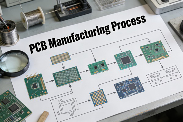
Table of Contents
Overview of the PCB Manufacturing Process
Although PCB complexity can vary, most rigid PCBs follow the same core manufacturing flow:
- Inner layer fabrication
- Layer alignment and lamination
- Drilling
- Copper plating
- Outer layer imaging and etching
- Solder mask application
- Surface finish
- Silkscreen printing
- Electrical testing and final inspection
Each step directly affects quality, yield, and cost.
Step 1 – Inner Layer Fabrication
Inner Layer Imaging
Manufacturing begins with copper-clad laminate sheets. The desired circuit pattern is transferred onto the copper surface using a photoresist and UV exposure.
Key factors:
- Trace width and spacing accuracy
- Photo alignment precision
- Cleanroom environment
Inner Layer Etching
Unwanted copper is chemically etched away, leaving the required circuit traces.
From a manufacturing perspective:
- Finer traces increase etching difficulty
- Over-etching or under-etching affects yield
At TOPFAST, inner layer etching parameters are optimised to balance precision and production stability.
Step 2 – Layer Alignment and Lamination
For multilayer PCBs, inner layers are stacked with prepreg and outer copper foils.
Lamination Process
- Heat and pressure bond all layers together
- Precise alignment ensures accurate via connections
Cost and quality impact:
- More layers increase lamination cycles
- Sequential lamination raises complexity and cost
Step 3 – Drilling
Drilling creates holes for vias and component leads.
Mechanical Drilling
Used for:
- Through-hole vias
- Larger hole sizes
Drilling cost increases with:
- Smaller hole diameters
- Higher aspect ratios
- High drill counts
Laser Drilling (Advanced PCBs)
Laser drilling is used for:
- Microvias in HDI PCBs
This process requires specialised equipment and increases manufacturing cost.
Step 4 – Copper Plating
After drilling, the holes must be electrically conductive.
Electroless Copper Deposition
A thin copper layer is deposited inside drilled holes to enable an electrical connection between layers.
Electroplating
Additional copper is plated to:
- Strengthen vias
- Achieve the required copper thickness
Plating uniformity directly affects reliability, especially for high-current or high-reliability applications.
Step 5 – Outer Layer Imaging and Etching
The outer layer circuit pattern is formed using a process similar to inner layers.
Key challenges:
- Maintaining trace accuracy after plating
- Controlling copper thickness
- Preventing shorts or opens
Outer layer processing has a major impact on final yield.
Step 6 – Solder Mask Application
Purpose of Solder Mask
Solder mask:
- Protects copper traces
- Prevents solder bridging
- Improves electrical insulation
Common colours include green, black, blue, and red. Green remains the most cost-effective and widely used option.
Solder Mask Quality Factors
- Registration accuracy
- Mask thickness
- Opening definition
Poor solder mask quality can cause assembly defects later.
Step 7 – Surface Finish
Surface finish protects exposed copper pads and ensures solderability.
Common Surface Finish Options
- HASL: Cost-effective, widely used
- ENIG: Flat surface, higher reliability
- OSP: Low cost, limited shelf life
TOPFAST recommends surface finishes based on application requirements rather than default preferences.
Step 8 – Silkscreen Printing
Silkscreen adds:
- Component reference designators
- Polarity markings
- Logos or identifiers
While not electrically functional, a clear silkscreen improves assembly accuracy and maintenance.
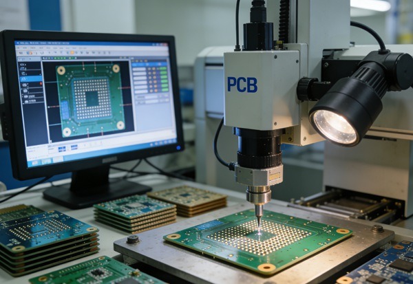
Step 9 – Electrical Testing and Final Inspection
Electrical Testing
Electrical testing verifies:
- Continuity
- Isolation
- Absence of shorts and open
This step is essential for ensuring functional reliability.
Final Quality Inspection
Final inspection may include:
- Visual inspection
- AOI (Automated Optical Inspection)
- Dimensional checks
At TOPFAST, inspection standards are aligned with IPC requirements and customer specifications.
How the PCB Manufacturing Process Affects Cost and Quality
Every manufacturing step introduces:
- Process variability
- Yield considerations
- Cost implications
Common cost drivers include:
- High layer counts
- Small drill sizes
- Tight tolerances
- Advanced surface finishes
Understanding the full process allows designers to optimise PCB designs for both cost and manufacturability.
Manufacturer’s Perspective: How TOPFAST Optimises PCB Manufacturing
As a PCB manufacturer, TOPFAST focuses on:
- Process standardization
- Early DFM feedback
- Yield-driven decision making
- Stable and scalable production
Rather than pushing unnecessary advanced processes, TOPFAST emphasises manufacturing-friendly designs that deliver consistent quality.
Conclusion
The PCB manufacturing process is a carefully controlled sequence of steps, each contributing to the final board’s performance, reliability, and cost.
By understanding how PCBs are made—from inner layer fabrication to final inspection—engineers and buyers can make better design and sourcing decisions.
With a manufacturing-first approach, TOPFAST helps customers turn complex designs into reliable, cost-effective PCBs.
PCB Step-by-Step Manufacturing Process FAQ
A: Standard PCB manufacturing typically takes 5–10 working days, depending on complexity and quantity.
A: Each step is important, but drilling and plating are critical for electrical reliability.
A: Yes. Multilayer PCBs require additional lamination and alignment steps.
A: Yes. Designs aligned with manufacturing capabilities improve yield and reduce cost.
A: TOPFAST uses standardised processes, DFM review, and comprehensive inspection to ensure consistent quality.