PCB manufacturing is a multi-step, tightly controlled process where small deviations can lead to reliability issues, yield loss, or increased cost.
While many resources describe PCB fabrication at a high level, understanding how each manufacturing step interacts with the next is critical for:
- Designing manufacturable boards
- Controlling cost
- Ensuring long-term reliability
This article provides a step-by-step overview of the PCB manufacturing process, with links to in-depth explanations of each critical stage.
The perspective reflects real manufacturing practices used by professional PCB manufacturers such as TOPFAST, where process stability and yield control are core priorities.
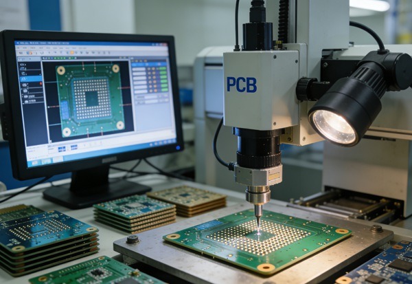
Table of Contents
Overview of the PCB Manufacturing Process
A typical PCB manufacturing workflow includes:
- Inner layer fabrication
- Drilling (mechanical or laser)
- Copper plating
- Pattern etching
- Inspection and yield control
Each step builds upon the previous one. Errors early in the process often cannot be corrected later.
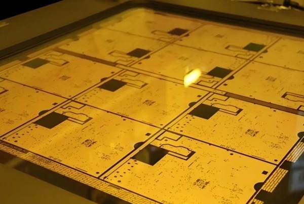
Inner Layer Fabrication
Inner layer fabrication is the foundation of multilayer PCB manufacturing.
At this stage:
- Copper foil is patterned to form internal circuits
- Dimensional accuracy is critical
- Defects are permanently locked into the stack after lamination
Because inner layers cannot be repaired once laminated, manufacturers apply strict process controls and inspection standards.
For a detailed explanation of inner layer preparation, imaging, and etching, see:
Inner Layer Fabrication Explained
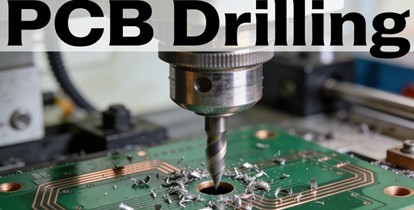
PCB Drilling: Creating Interlayer Connections
Drilling creates the holes that will later become vias and through-hole connections.
Two primary drilling methods are used:
- Mechanical drilling
- Laser drilling
Each method has trade-offs in:
- Hole size
- Aspect ratio
- Cost
- Reliability
Improper drilling directly affects plating quality and via reliability.
To understand when mechanical drilling or laser drilling is appropriate, read:
PCB Drilling vs. Laser Drilling
Copper Plating Process
Copper plating transforms drilled holes into electrically conductive vertical connections.
The plating process includes:
- Electroless copper deposition
- Electrolytic copper thickness build-up
Plating quality determines:
- Via wall strength
- Thermal cycling performance
- Current-carrying capability
Inconsistent plating is a common root cause of field failures, even when boards pass initial electrical tests.
For a full breakdown of plating stages and reliability considerations, see:
Copper Plating Process in PCB Manufacturing Explained
PCB Etching and Circuit Formation
Etching removes unwanted copper to define the final circuit pattern.
This step must balance:
- Copper thickness
- Line width accuracy
- Spacing control
Over-etching or under-etching leads to:
- Opens or shorts
- Impedance variation
- Reduced manufacturing yield
Etching performance becomes increasingly critical as designs move toward finer traces and higher layer counts.
For an in-depth look at etching chemistry and yield impact, read:
PCB Etching Process and Yield Control Explained
Yield Control Across the Manufacturing Process
Yield is not controlled at a single step—it is the result of cumulative process stability.
Key yield drivers include:
- Inner layer accuracy
- Drill quality
- Plating uniformity
- Etching consistency
Professional PCB manufacturers continuously monitor yield data to:
- Identify process drift
- Optimize design rules
- Reduce scrap and rework
At TOPFAST, yield feedback is integrated into DFM reviews to help customers avoid hidden manufacturing risks before production begins.
For a manufacturing-focused overview of yield drivers, see:
PCB Etching Process and Yield Control Explained
How Design Decisions Affect the Manufacturing Process
From a manufacturing standpoint, many PCB issues originate in design choices such as:
- Excessively fine trace widths
- High aspect ratio vias
- Unbalanced copper distribution
- Overly tight tolerances
Early collaboration between designers and manufacturers helps align design intent with process capability.
This approach reduces:
- Iterations
- Production delays
- Total cost of ownership
Manufacturer’s Perspective: Process Integration at TOPFAST
As a professional PCB manufacturer, TOPFAST approaches PCB fabrication as an integrated system, not isolated steps.
Key principles include:
- Stable process windows
- Early DFM risk identification
- Yield-driven optimization
- IPC-aligned quality standards
Rather than focusing solely on minimum specifications, the emphasis is on repeatability, reliability, and scalable production.
Conclusion
The PCB manufacturing process is a sequence of interdependent steps where quality is built progressively, not inspected at the end.
By understanding how inner layer fabrication, drilling, copper plating, and etching work together, engineers and buyers can:
- Make better design decisions
- Reduce manufacturing risk
- Control cost without sacrificing quality
This overview serves as a gateway to deeper technical explanations of each critical stage, reflecting real-world practices used by experienced PCB manufacturers like TOPFAST.