Table of Contents
PCB SBU Industry Insight
Strategic Position & Market Value
As the “central nervous system” of electronics, printed circuit boards (PCBs) hold irreplaceable importance in modern manufacturing. According to Prismark, the global PCB market exceeded $80 billion in 2023, with a steady CAGR of 5.8%. Driven by 5G, AIoT, and electric vehicles, PCB Strategic Business Units (SBUs) are evolving from passive components into strategic innovation drivers.
PCB SBU Core Value
1.Supply Chain Nexus
Upstream: Specialized materials (high-frequency PTFE, ABF substrates for IC packaging)
Downstream: Six key sectors—consumer electronics (32%), telecom (28%), automotive (18%), medical (11%), industrial (8%), and aerospace (3%)
2.End-to-End Solutions
Co-design: Signal integrity optimization (<0.1dB loss via SI/PI simulation)
Smart manufacturing: mSAP process enabling 20/20μm line/space precision
Supply chain efficiency: Panel-level production (18×24 in standard) boosts material utilization to 93%
3.Production Optimization
| Unit | Focus | Efficiency Gain |
|---|---|---|
| PCS | Miniaturization | 0201 component assembly |
| SET | Modular integration | 40% faster testing |
| PANEL | Scalability | 25% cost reduction |
Technology Breakthroughs
1.Advanced PCB Technologies
HDI: Stacked microvias for 16-layer interconnects
Flexible circuits: 3D-MID for wearable medical devices
High-frequency materials: Ceramic composites with Dk <3.0 / Df <0.002
2.Industry 4.0 Transformation
AI-powered AOI achieves 99.98% defect detection
Digital twin slashes NPI cycles to 72 hours
Hydrogen-based curing cuts energy use by 35%
Competitive Strategy & Future Roadmap
Key Challenges
Dual-supply chain for copper foil/resin (geopolitical resilience)
Bio-degradable substrates for EU RoHS 3.0 compliance
Growth Engines
Southeast Asia hub: Vietnam facility for automotive PCB localization
Heterogeneous integration: 2.5D/3D substrates with 5μm line width
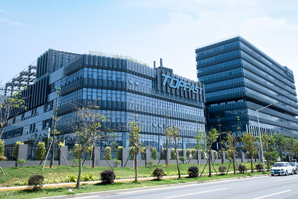
Topfast’s Competitive Edge
As an IATF 16949-certified leader, we deliver three pillars of excellence
1. Technology Leadership
Capable of mass production of SLP 10μm lines.
Semiconductor test boards (±25μm tolerance)
2.Operational Reliability
24-hour prototyping (vs. industry-standard 72 hours)
99.2% on-time delivery for high-volume orders
3. Ecosystem Partnerships
DFM analysis + testing integration
Lifetime traceability with client-dedicated tech archives
Our “Concept-to-Production” approach powers mission-critical applications, from SpaceX Starlink terminals to Da Vinci surgical robots. With 8.7% R&D investment, we lead in materials science and precision engineering.
The Next Frontier
As silicon photonics and terahertz communications emerge, Topfast is pioneering:
Optical PCBs: Co-packaged photonic components
Nanocellulose substrates: 60% lower carbon footprint
Quantum interconnects: Cryogenic superconducting bonding
By fusing craftsmanship with digital intelligence, we’re redefining connectivity standards. Partner with Topfast to build the future of electronics.