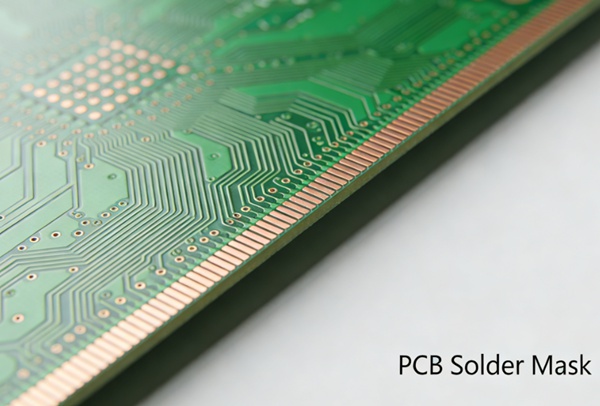
Solder mask is one of the most visible layers on a printed circuit board. It covers the copper traces while leaving component pads exposed for soldering.
Although the solder mask appears simple, improper design can lead to several manufacturing and assembly problems, including:
- solder bridges between pads
- poor solder joints
- exposed copper areas
- Reduced PCB yield
Following proper PCB solder mask design guidelines ensures that the mask layer supports both fabrication and assembly processes.
This guide explains the key design parameters engineers should consider when creating solder mask openings and clearances.
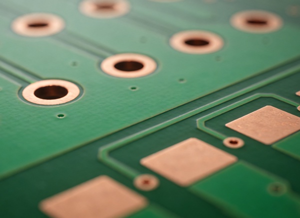
Table of Contents
What Is PCB Solder Mask?
Solder mask is a polymer coating applied to PCB surfaces to protect copper traces and prevent unintended solder connections.
Its main functions include:
- protecting copper from oxidation
- preventing solder bridging
- improving insulation between conductors
- enhancing PCB appearance
During PCB fabrication, the solder mask layer is applied after copper pattern formation and before surface finishing.
The overall fabrication workflow is explained in: PCB Manufacturing Process Explained
Types of Solder Mask
Several types of solder mask are used in PCB manufacturing.
Liquid Photoimageable Solder Mask (LPI)
The most common type used in modern PCBs.
Characteristics:
- applied as a liquid coating
- patterned using photolithography
- supports fine-pitch components
Dry Film Solder Mask
Less commonly used but suitable for specific applications.
Features:
- laminated film
- uniform thickness
- Good for high-precision designs
Epoxy Screen-Printed Mask
Used mainly in older or low-cost PCB processes.
Limitations:
- lower resolution
- not suitable for fine-pitch components
Key PCB Solder Mask Design Rules
Several design parameters influence solder mask performance.
1. Solder Mask Clearance
Solder mask clearance defines the distance between the copper pad edge and the mask opening.
Typical guideline:
Mask clearance: 3–4 mil
Adequate clearance ensures that pads are fully exposed during assembly.
If clearance is too small:
- The mask may cover the pad edges
- Solder joints may be unreliable
2. Solder Mask Expansion
Mask expansion is the amount by which the solder mask opening is enlarged beyond the copper pad.
Example:
Pad size = 20 mil
Mask opening = 24 mil
Expansion = 2 mil per side
This expansion compensates for mask alignment tolerances during fabrication.
3. Solder Mask Dam Width
The solder mask dam is the narrow strip of mask between two pads.
Typical minimum dam width:
≥ 4 mil
If the dam is too narrow, it may break during manufacturing, increasing the risk of solder bridges.
4. Fine-Pitch Component Considerations
Fine-pitch ICs and BGAs require a special solder mask design.
Common approaches include:
Solder Mask Defined Pads (SMD)
Mask opening defines pad size.
Advantages:
- tighter control for small components
Non-Solder Mask Defined Pads (NSMD)
The copper pad defines the size, mask opening is larger.
Advantages:
- better solder joint reliability
- commonly used for BGA pads

How to Design PCB Solder Mask (Practical Steps)
Engineers typically follow several steps when defining solder mask rules.
- Step 1 — Define mask expansion rules
Set the global mask expansion in the PCB design software.
Typical range: 2–4 mil - Step 2 — Check fine-pitch components
Verify solder mask openings around:
QFN
BGA
small pitch connectors - Step 3 — Verify mask dam widths
Ensure spacing between adjacent pads can support mask dams.
- Step 4 — Perform DFM checks
Manufacturers review solder mask data to ensure manufacturability.
The DFM review process is described in: PCB DFM Checklist Before Sending Gerber Files
Common PCB Solder Mask Design Mistakes
Several design issues frequently appear in PCB layouts.
Mask openings are too small
May partially cover pads.
Insufficient solder mask dam
Leads to solder bridging.
Incorrect pad definitions
A mismatch between the mask and the copper pads can cause assembly issues.
Ignoring manufacturing tolerances
Mask alignment tolerances must be considered.
Many reliability issues during assembly originate from design problems discussed in: Common PCB Failures and Reliability Issues
Manufacturing Considerations
PCB manufacturers evaluate solder mask layers during CAM analysis.
They review:
- mask openings
- mask clearance
- dam widths
- alignment tolerances
At manufacturers such as TOPFAST, engineering teams typically verify solder mask parameters before fabrication to ensure compatibility with both PCB fabrication and assembly processes.
Conclusion
Solder mask design plays a crucial role in PCB manufacturability and assembly reliability.
By following practical design rules—such as proper mask clearance, sufficient dam width, and correct pad definitions—engineers can reduce assembly defects and improve production yield.
Close coordination between design teams and PCB manufacturers also helps ensure solder mask layers meet fabrication capabilities.
PCB Solder Mask FAQ
A: Solder mask clearance is the distance between the copper pad edge and the solder mask opening, ensuring pads remain exposed during assembly.
A: Most PCB manufacturers recommend a minimum solder mask dam width of 4 mil to prevent mask breakage.
A: Small mask openings may partially cover pads, resulting in poor solder joints.
A: SMD pads are defined by solder mask openings, while NSMD pads are defined by the copper pad itself. NSMD pads are commonly used for BGA components.