Gedruckte Schaltungen (PCBs) sind die Grundlage moderner elektronischer Produkte. Während sich viele Ingenieure auf das Design von Leiterplatten konzentrieren, verstehen weniger wie eine Leiterplatte tatsächlich hergestellt wird.
Das Verständnis des PCB-Herstellungsprozesses ist hilfreich:
- Verbesserung des Designs für die Herstellbarkeit (DFM)
- Senkung der Produktionskosten
- Vermeiden Sie Qualitätsprobleme
- Effektivere Kommunikation mit PCB-Herstellern
Dieser Artikel enthält eine klare, schrittweise Erklärung des PCB-Herstellungsprozessesbasierend auf realen Produktionspraktiken, die von TOPFASTein professioneller Leiterplattenhersteller, der Prototypen und Massenproduktion unterstützt.
Inhaltsübersicht
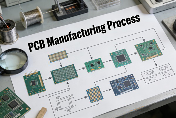
Überblick über den PCB-Herstellungsprozess
Obwohl die Komplexität von Leiterplatten variieren kann, folgen die meisten starren Leiterplatten demselben Kernherstellungsablauf:
- Herstellung der inneren Schicht
- Lagenausrichtung und Laminierung
- Bohren
- Verkupfern
- Bebilderung und Ätzung der Außenschicht
- Aufbringen der Lötmaske
- Oberflächengüte
- Siebdruck
- Elektrische Prüfung und Endkontrolle
Jeder Schritt hat direkte Auswirkungen auf Qualität, Ertrag und Kosten.
Schritt 1 - Herstellung der inneren Schicht
Inner Layer Imaging
Die Herstellung beginnt mit kupferkaschierten Laminatplatten. Das gewünschte Schaltungsmuster wird mit einem Fotolack und UV-Belichtung auf die Kupferoberfläche übertragen.
Schlüsselfaktoren:
- Leiterbahnbreite und Abstandsgenauigkeit
- Präzision der Fotoausrichtung
- Reinraumumgebung
Ätzen der inneren Schicht
Unerwünschtes Kupfer wird chemisch weggeätzt, so dass die erforderlichen Leiterbahnen übrig bleiben.
Aus der Perspektive der Herstellung:
- Feinere Spuren erschweren das Ätzen
- Über- oder Unterätzung beeinträchtigt die Ausbeute
Bei TOPFAST werden die Parameter für das Ätzen von Innenschichten so optimiert, dass ein Gleichgewicht zwischen Präzision und Produktionsstabilität.
Schritt 2 - Lagenausrichtung und Kaschierung
Bei mehrlagigen Leiterplatten werden die inneren Lagen mit Prepreg und äußeren Kupferfolien gestapelt.
Lamination Prozess
- Hitze und Druck verbinden alle Schichten miteinander
- Präzise Ausrichtung gewährleistet exakte Via-Verbindungen
Auswirkungen auf Kosten und Qualität:
- Mehr Schichten erhöhen die Laminierzyklen
- Sequenzielle Laminierung erhöht die Komplexität und die Kosten
Schritt 3 - Bohren
Durch das Bohren entstehen Löcher für Durchkontaktierungen und Bauteilanschlüsse.
Mechanisches Bohren
Verwendet für:
- Durchgangsloch-Vias
- Größere Lochgrößen
Die Bohrkosten steigen mit:
- Kleinere Lochdurchmesser
- Höhere Seitenverhältnisse
- Hohe Anzahl von Bohrungen
Laserbohren (Advanced PCBs)
Laserbohren wird eingesetzt für:
- Microvias in HDI-Leiterplatten
Dieses Verfahren erfordert spezielle Ausrüstung und erhöht die Herstellungskosten.
Schritt 4 - Verkupfern
Nach dem Bohren müssen die Löcher elektrisch leitfähig sein.
Stromlose Kupferabscheidung
In den Bohrlöchern wird eine dünne Kupferschicht aufgebracht, um eine elektrische Verbindung zwischen den Schichten herzustellen.
Galvanik
Zusätzliches Kupfer wird aufplattiert:
- Durchkontaktierungen verstärken
- Erreichen der erforderlichen Kupferdicke
Die Gleichmäßigkeit der Beschichtung wirkt sich direkt auf die Zuverlässigkeit aus, insbesondere bei Anwendungen mit hohen Strömen oder hoher Zuverlässigkeit.
Schritt 5 - Bebilderung und Ätzung der Außenschicht
Die äußere Schaltungsstruktur wird in einem ähnlichen Verfahren wie die inneren Schichten hergestellt.
Die wichtigsten Herausforderungen:
- Aufrechterhaltung der Spurengenauigkeit nach der Beschichtung
- Kontrolle der Kupferdicke
- Verhinderung von Kurzschlüssen oder Öffnungen
Die Verarbeitung der Außenschicht hat einen großen Einfluss auf endgültige Rendite.
Schritt 6 - Aufbringen der Lötstoppmaske
Zweck der Lötstoppmaske
Lötmaske:
- Schützt Kupferspuren
- Verhindert die Bildung von Lötbrücken
- Verbessert die elektrische Isolierung
Zu den gängigen Farben gehören Grün, Schwarz, Blau und Rot. Grün ist nach wie vor die kostengünstigste und am weitesten verbreitete Option.
Qualitätsfaktoren für Lötmasken
- Genauigkeit der Registrierung
- Dicke der Maske
- Definition der Eröffnung
Eine schlechte Qualität der Lötmaske kann später zu Montagefehlern führen.
Schritt 7 - Oberflächenbehandlung
Die Oberflächenbehandlung schützt die freiliegenden Kupferpads und gewährleistet die Lötbarkeit.
Gemeinsame Optionen für die Oberflächenausführung
- HASL: Kostengünstig, weit verbreitet
- ENIG: Flache Oberfläche, höhere Zuverlässigkeit
- OSP: Geringe Kosten, begrenzte Haltbarkeit
TOPFAST empfiehlt Oberflächenbehandlungen auf der Grundlage von Anwendungsanforderungen und nicht Standardeinstellungen.
Schritt 8 - Siebdruck
Siebdruck fügt hinzu:
- Referenzbezeichner für Komponenten
- Kennzeichnung der Polarität
- Logos oder Erkennungszeichen
Ein klarer Siebdruck ist zwar nicht elektrisch funktionsfähig, verbessert aber die Montagegenauigkeit und die Wartung.
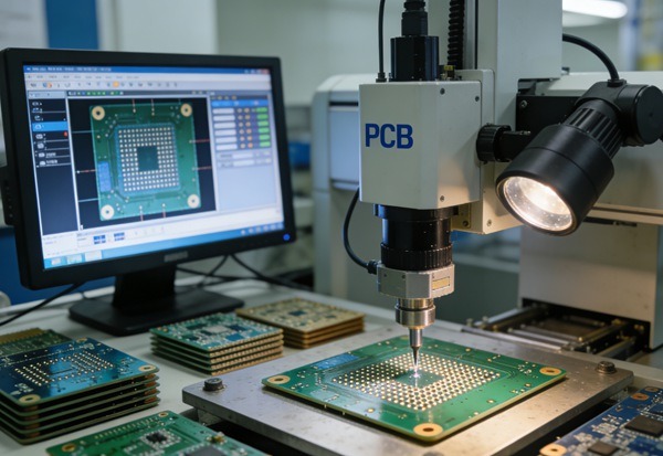
Schritt 9 - Elektrische Prüfung und Abschlussinspektion
Elektrische Prüfung
Die elektrische Prüfung verifiziert:
- Kontinuität
- Isolierung
- Fehlen von kurzen Hosen und offenen
Dieser Schritt ist für die Gewährleistung der Funktionssicherheit unerlässlich.
Abschließende Qualitätsprüfung
Die Endkontrolle kann Folgendes umfassen:
- Visuelle Kontrolle
- AOI (Automatisierte optische Inspektion)
- Maßkontrollen
Bei TOPFAST sind die Inspektionsstandards abgestimmt auf IPC-Anforderungen und Kundenspezifikationen.
Wie sich der PCB-Herstellungsprozess auf Kosten und Qualität auswirkt
Jeder Fertigungsschritt führt zu:
- Prozessvariabilität
- Überlegungen zur Rendite
- Auswirkungen auf die Kosten
Zu den üblichen Kostentreibern gehören:
- Hohe Schichtzahlen
- Kleine Bohrergrößen
- Enge Toleranzen
- Fortschrittliche Oberflächenveredelung
Das Verständnis des gesamten Prozesses ermöglicht es Designern Optimierung von PCB-Designs im Hinblick auf Kosten und Herstellbarkeit.
Herstellerperspektive: Wie TOPFAST die PCB-Herstellung optimiert
Als PCB-Hersteller konzentriert sich TOPFAST auf:
- Standardisierung von Prozessen
- Frühes DFM-Feedback
- Renditeorientierte Entscheidungsfindung
- Stabile und skalierbare Produktion
Anstatt unnötige fortgeschrittene Prozesse zu forcieren, legt TOPFAST Wert auf fertigungsfreundliche Designs, die gleichbleibende Qualität liefern.
Schlussfolgerung
Der Herstellungsprozess von Leiterplatten ist eine sorgfältig kontrollierte Abfolge von Schritten, von denen jeder einzelne zur Leistung, Zuverlässigkeit und zu den Kosten der fertigen Leiterplatte beiträgt.
Wenn man versteht, wie Leiterplatten hergestellt werden - von der Herstellung der Innenlagen bis zur Endkontrolle - können Ingenieure und Einkäufer bessere Design- und Beschaffungsentscheidungen treffen.
Mit einem Ansatz, bei dem die Fertigung im Vordergrund steht, TOPFAST hilft Kunden, komplexe Designs in zuverlässige, kosteneffektive PCBs zu verwandeln.
PCB Schritt-für-Schritt-Herstellungsprozess FAQ
A: Die Standard-PCB-Fertigung dauert in der Regel 5-10 Arbeitstage, je nach Komplexität und Menge.
A: Jeder Schritt ist wichtig, aber Bohren und Beschichten sind entscheidend für die elektrische Zuverlässigkeit.
A: Ja. Bei mehrlagigen Leiterplatten sind zusätzliche Laminierungs- und Ausrichtungsschritte erforderlich.
A: Ja. Auf die Fertigungsmöglichkeiten abgestimmte Designs verbessern die Ausbeute und senken die Kosten.
A: TOPFAST verwendet standardisierte Prozesse, DFM-Überprüfung und umfassende Inspektionen, um eine gleichbleibende Qualität zu gewährleisten.