La fabricación de placas de circuito impreso es proceso en varios pasos, estrictamente controlado donde pequeñas desviaciones pueden provocar problemas de fiabilidad, pérdidas de rendimiento o un aumento de los costes.
Aunque muchos recursos describen la fabricación de placas de circuito impreso a un alto nivel, la comprensión cómo interactúa cada fase de fabricación con la siguiente es fundamental para:
- Diseño de placas fabricables
- Control de costes
- Fiabilidad a largo plazo
Este artículo ofrece una descripción paso a paso del proceso de fabricación de placas de circuito impresocon enlaces a explicaciones detalladas de cada etapa crítica.
La perspectiva refleja prácticas de fabricación reales utilizadas por fabricantes profesionales de placas de circuito impreso como TOPFASTdonde la estabilidad del proceso y el control del rendimiento son prioridades básicas.
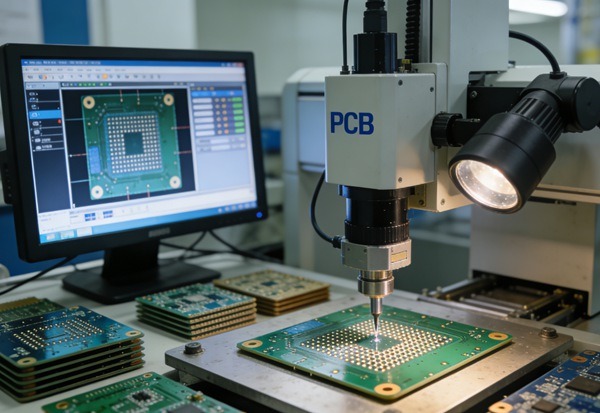
Tabla de contenidos
Visión general de la Proceso de fabricación de PCB
Un flujo de trabajo típico de fabricación de placas de circuito impreso incluye:
- Fabricación de la capa interior
- Taladrado (mecánico o láser)
- Cobreado
- Grabado de patrones
- Inspección y control del rendimiento
Cada paso se basa en el anterior. Los errores cometidos al principio del proceso no suelen poder corregirse después.
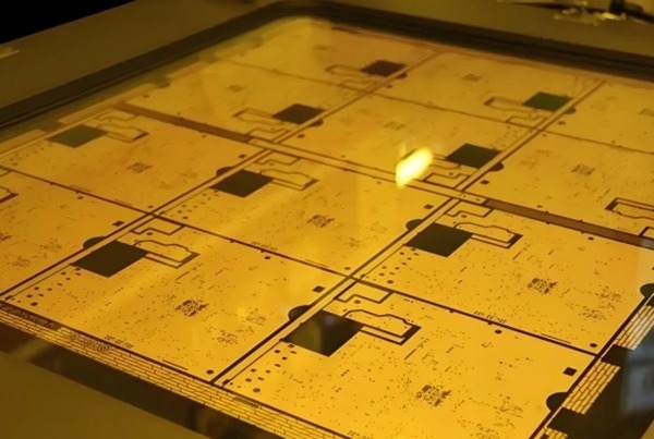
Fabricación de la capa interior
La fabricación de la capa interior es el cimientos de la fabricación de placas de circuito impreso multicapa.
En esta etapa:
- La lámina de cobre se estampa para formar circuitos internos
- La precisión dimensional es fundamental
- Los defectos quedan fijados permanentemente en la pila tras la laminación
Dado que las capas internas no pueden repararse una vez laminadas, los fabricantes aplican estrictos controles de proceso y normas de inspección.
Para una explicación detallada de la preparación de la capa interna, la obtención de imágenes y el grabado, véase:
Explicación de la fabricación de la capa interior
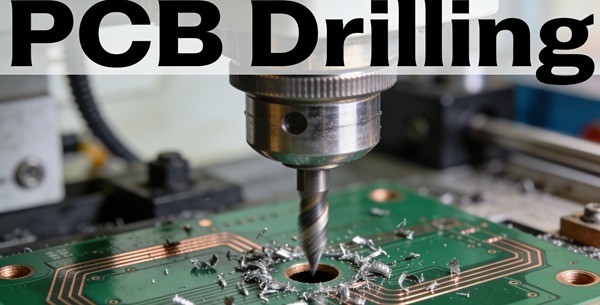
Taladrado de PCB: Creación de conexiones entre capas
El taladrado crea los orificios que más tarde se convertirán en vías y conexiones pasantes.
Se utilizan dos métodos principales de perforación:
- Perforación mecánica
- Taladrado láser
Cada método tiene sus ventajas e inconvenientes:
- Tamaño del orificio
- Relación de aspecto
- costo
- Fiabilidad
Un taladrado incorrecto afecta directamente a la calidad del chapado y a la fiabilidad de la vía.
Para saber cuándo es adecuado el taladrado mecánico o el taladrado láser, lea:
Taladrado de placas de circuito impreso vs. Taladrado láser
Proceso de cobreado
El cobreado transforma los orificios perforados en conexiones verticales conductoras de electricidad.
El proceso de revestimiento incluye:
- Deposición de cobre químico
- Acumulación de espesor de cobre electrolítico
La calidad del chapado determina:
- A través de la resistencia de la pared
- Rendimiento en ciclos térmicos
- Capacidad de transporte de corriente
El revestimiento inconsistente es una causa común de fallos de campo, incluso cuando las placas superan las pruebas eléctricas iniciales.
Para un desglose completo de las etapas de revestimiento y consideraciones de fiabilidad, véase:
Explicación del proceso de cobreado en la fabricación de placas de circuito impreso
Grabado de PCB y formación de circuitos
El grabado elimina el cobre no deseado para definir el patrón final del circuito.
Este paso debe equilibrarse:
- Espesor del cobre
- Precisión del ancho de línea
- Control del espacio
Un grabado excesivo o insuficiente provoca:
- Abiertos o cortos
- Variación de impedancia
- Reducción del rendimiento de fabricación
El rendimiento del grabado es cada vez más crítico a medida que los diseños avanzan hacia trazas más finas y un mayor número de capas.
Para conocer en profundidad la química del grabado y el impacto en el rendimiento, lea:
Explicación del proceso de grabado de PCB y del control de rendimiento
Control del rendimiento en todo el proceso de fabricación
El rendimiento no se controla en un solo paso: es el resultado de la estabilidad acumulada del proceso.
Los principales factores de rendimiento son:
- Precisión de la capa interna
- Calidad de perforación
- Uniformidad del revestimiento
- Consistencia del grabado
Los fabricantes profesionales de placas de circuito impreso controlan continuamente los datos de rendimiento para:
- Identificar la desviación del proceso
- Optimizar las reglas de diseño
- Reducir las piezas desechadas y los reprocesamientos
En TOPFAST, la información sobre el rendimiento se integra en las revisiones DFM para ayudar a los clientes a evitar riesgos de fabricación ocultos antes de que comience la producción.
Para una visión general de los factores de rendimiento centrada en la fabricación, véase:
Explicación del proceso de grabado de PCB y del control de rendimiento
Cómo afectan las decisiones de diseño al proceso de fabricación
Desde el punto de vista de la fabricación, muchos problemas de las placas de circuito impreso tienen su origen en decisiones de diseño como:
- Ancho de trazo excesivamente fino
- Vías de alta relación de aspecto
- Distribución de cobre desequilibrada
- Tolerancias demasiado estrechas
La colaboración temprana entre diseñadores y fabricantes ayuda a alinear la intención del diseño con la capacidad del proceso.
Este enfoque reduce:
- Iteraciones
- Retrasos en la producción
- Coste total de propiedad
Perspectiva del fabricante: Integración de procesos en TOPFAST
Como fabricante profesional de PCB, TOPFAST aborda la fabricación de PCB como un sistema integradono pasos aislados.
Entre los principios clave figuran:
- Ventanas de proceso estables
- Identificación precoz de los riesgos de DFM
- Optimización en función del rendimiento
- Normas de calidad alineadas con IPC
En lugar de centrarse únicamente en las especificaciones mínimas, se hace hincapié en repetibilidad, fiabilidad y producción escalable.
Conclusión
El proceso de fabricación de PCB es una secuencia de pasos interdependientes en la que la calidad se construye progresivamente, no se inspecciona al final.
Los ingenieros y compradores pueden comprender cómo funcionan conjuntamente la fabricación de capas internas, el taladrado, el cobreado y el grabado:
- Tome mejores decisiones de diseño
- Reducir el riesgo de fabricación
- Controle los costes sin sacrificar la calidad
Esta visión general sirve como puerta de entrada a explicaciones técnicas más profundas de cada etapa crítica, reflejando las prácticas del mundo real utilizadas por fabricantes experimentados de placas de circuito impreso como TOPFAST.