Descrizione
Nella moderna produzione elettronica, la qualità dell'assemblaggio di PCB industriali determina direttamente le prestazioni e l'affidabilità del prodotto finale. In qualità di fornitore unico di soluzioni PCB con 17 anni di esperienza nel settore, comprendiamo a fondo i severi requisiti delle applicazioni industriali per l'assemblaggio dei circuiti stampati: dall'affidabilità assoluta per i dispositivi medici alla stabilità a lungo termine per i sistemi di controllo industriali, dall'adattabilità ambientale per l'elettronica automobilistica alle prestazioni estreme per il settore aerospaziale. Questo articolo esplorerà le tecnologie chiave, il controllo di qualità e le applicazioni industriali dell'assemblaggio di circuiti stampati, mostrando come la moderna produzione elettronica raggiunga il perfetto equilibrio tra funzionalità e affidabilità attraverso processi di precisione.
Indice per materie
Vantaggi tecnologici fondamentali dell'assemblaggio industriale di PCB
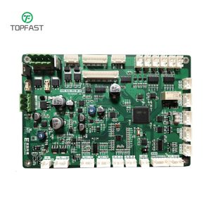
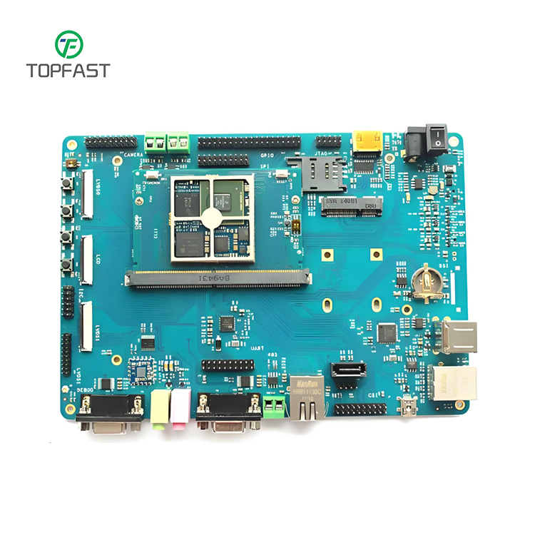
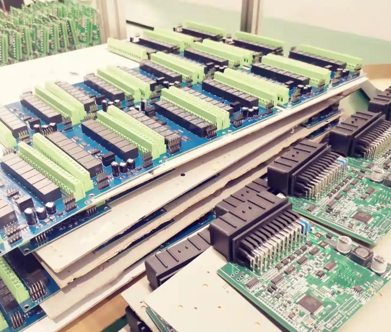
Nell'industria elettronica in rapida crescita, l'assemblaggio industriale di PCB si è evoluto dal semplice montaggio dei componenti a un progetto sistematico che integra scienza dei materiali, macchinari di precisione e controllo dell'automazione. Le linee di produzione SMT completamente automatizzate costruite nei nostri stabilimenti sono in grado di ottenere una qualità costante per milioni di giunti di saldatura all'ora, grazie alla sinergia di tre pilastri tecnologici fondamentali.
1. Tecnologia di montaggio ad alta precisione
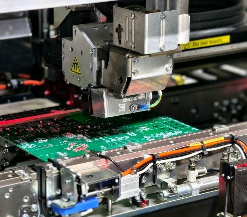
È la prima barriera di qualità per l'assemblaggio di PCB industriali. La nostra macchina di posizionamento multifunzionale è dotata di un sistema di posizionamento a visione submicronica, in grado di gestire con precisione diversi requisiti di componenti che vanno dai componenti ultra-miniaturizzati 01005 (0,4 mm x 0,2 mm) ai BGA di grandi dimensioni (45 mm x 45 mm). Nella produzione effettiva, la precisione di posizionamento raggiunge ±25μm (CPK≥1,67) e l'offset dei componenti è rigorosamente controllato entro 15% della larghezza della piazzola, un valore di gran lunga superiore ai requisiti standard del settore di 25%. Questa precisione garantisce l'integrità della trasmissione dei segnali ad alta frequenza e le prestazioni di dissipazione del calore dei dispositivi di potenza.
2. Sistemi intelligenti di controllo del processo di saldatura
Costituisce la base per una connessione elettrica affidabile. Il nostro forno di riflusso schermato con azoto a 10 zone di temperatura è dotato di un sistema di rilevamento della temperatura in tempo reale che ottimizza automaticamente il profilo di temperatura per le diverse leghe di pasta saldante (SAC305, SnBi58, ecc.) e i materiali dei PCB (alto TG, substrati ceramici, ecc.). I dati effettivi dimostrano che il sistema è in grado di controllare il tasso di difetti di saldatura a <200DPPM (difetti per milione di punti), in particolare per i componenti QFN, LGA e altri bottom pad con una resa di saldatura di 99,98% o superiore.
3.Sistema tecnologico di ispezione 3D
Viene realizzato un controllo ad anello chiuso della qualità del processo. L'SPI (Solder Paste Inspection), l'AOI (Automatic Optical Inspection) e i raggi X 3D installati sulla linea di produzione formano il "triangolo della qualità": Il sistema SPI monitora la deviazione dello spessore della pasta saldante con una risoluzione di 5μm; l'apparecchiatura AOI riconosce le anomalie delle giunzioni di saldatura con una profondità di 0,02mm² grazie all'algoritmo di deep learning; e i raggi X possono visualizzare le connessioni interne del PCB a 56 strati. Questa strategia di ispezione multistrato ha portato a un tasso di rilevamento 98% dei problemi di processo precoci, riducendo drasticamente i costi di riparazione successivi.
Capacità di produzione di processo completa, dalla progettazione al collaudo
L'affidabilità dei dispositivi elettronici industriali inizia dalla fase di progettazione, prosegue attraverso il processo di produzione e termina con il collaudo. Il nostro **sistema di produzione a ciclo di vita completo** copre ogni punto critico, dal supporto alla progettazione alla produzione di massa, garantendo che i componenti PCB mantengano un funzionamento stabile a lungo termine in ambienti industriali difficili.
1. Fase di coottimizzazione del progetto
Il nostro team di ingegneri interviene in anticipo nel processo di progettazione del cliente per fornire analisi di producibilità (DFM) e raccomandazioni di progettazione per l'affidabilità (DFR). Grazie a un software di simulazione dedicato, siamo in grado di identificare i problemi di adattamento dell'impedenza nelle linee di segnale ad alta velocità, di prevedere la distribuzione del calore nel piano di alimentazione e di proporre soluzioni di ottimizzazione. Abbiamo assistito un cliente di un controllore industriale a ridurre il numero di iterazioni di progettazione da 5 a 2, abbreviando il ciclo di sviluppo di 40%. Questa collaborazione anticipata riduce significativamente i rischi di qualità nella produzione successiva.
2. Linea di produzione flessibile
Le linee di produzione flessibili possono rispondere contemporaneamente a esigenze produttive diversificate: le linee SMT a doppio binario consentono un rapido cambio di linea (<15 minuti) e supportano una produzione flessibile dai prototipi ai medi volumi (50-10.000 pezzi); le apparecchiature per la saldatura a onda selettiva possono controllare l'intervallo di shock termico dei componenti a foro passante oltre i 5 mm dei componenti vicini; il processo di rivestimento a tripla protezione controlla con precisione lo spessore del rivestimento tra 25-75μm per soddisfare i requisiti di diversi livelli di protezione. Il processo di rivestimento a tripla protezione controlla con precisione lo spessore del rivestimento tra 25-75μm per soddisfare diversi livelli di protezione. Questa capacità produttiva flessibile ci permette di servire clienti in diversi settori, come le apparecchiature mediche e l'automazione industriale, senza sacrificare l'efficienza produttiva o gli standard di qualità.
3. Sistema di verifica dell'affidabilità
Il sistema di verifica dell'affidabilità è il vantaggio principale che ci distingue dai comuni sistemi di controllo. Gruppo PCB fabbriche. Oltre ai tradizionali test ICT (in-circuit test) e FCT (functional test), abbiamo creato un laboratorio completo di Environmental Stress Screening (ESS) in grado di eseguire:
- Test dei cicli di temperatura (-55℃~+125℃, 100 cicli)
- Conservazione ad alta temperatura e umidità (85℃/85%RH, 1000 ore)
- Prova di vibrazione meccanica (5-500Hz, 30 minuti per ciascuno dei 3 assi)
- Test dei cicli di alimentazione (carico 0-100%, 10.000 volte)
Questi test rigorosi garantiscono l'affidabilità a lungo termine dei prodotti in ambienti industriali. La scheda di controllo di un progetto di transito ferroviario ha raggiunto oltre 50.000 ore di funzionamento senza guasti sul campo dopo aver superato i test.
Processi industriali speciali e soluzioni per i materiali
I dispositivi elettronici industriali devono spesso affrontare sfide ambientali estreme, come le alte temperature, l'elevata umidità, le vibrazioni e la corrosione, che sono difficili da affrontare con i comuni processi di assemblaggio di PCB di tipo consumer. Abbiamo sviluppato **Sistemi di processo speciali** che sono specializzati in queste condizioni difficili e forniscono soluzioni affidabili per applicazioni critiche.
1. Tecnologia di saldatura ad alta affidabilità
Abbiamo sviluppato una varietà di soluzioni per diversi scenari applicativi
- La tecnologia Copper Wire Bonding (CWB) viene utilizzata per connessioni ad alta corrente, sostituendo i metodi tradizionali di wire bonding e aumentando la capacità di trasporto della corrente fino a 300%.
- Sinterizzazione Ag per l'assemblaggio di moduli di potenza con temperature di esercizio fino a 200°C.
- Per i componenti sensibili al calore si utilizza la saldatura a bassa temperatura (SnBi58) e la finestra di processo è controllata entro ±3℃.
Questi processi hanno aumentato l'MTBF (Mean Time Between Failure) di un modulo di ricarica per veicoli elettrici da 50.000 ore a 150.000 ore.
2. Capacità di lavorazione di substrati speciali
Soddisfare le esigenze di varie applicazioni complesse
- Tecnologia di lavorazione del PCB in rame spesso (spessore del rame di 6 oz) per supportare la progettazione di alimentatori industriali ad alta corrente.
- Processo di stampaggio integrato Rigid-Flex (Rigid-Flex) per ridurre i punti di rottura dei connettori
- Trattamento della conducibilità termica del substrato metallico (IMS), per risolvere il problema della dissipazione del calore dei LED ad alta potenza
- Materiali ad alta frequenza (Rogers, Tecneli) lavorati con precisione, per garantire le prestazioni RF delle stazioni base 5G.
3. Per la corrosione chimica in ambienti industriali
Forniamo un programma di protezione a più livelli
- Tecnologia di nanorivestimento per formare una pellicola protettiva di 5-8μm che supera il test della nebbia salina di 96 ore.
- Processo di rivestimento conformale per ottenere una protezione a tre prove (umidità, muffa e nebbia salina).
- La tecnologia Potting viene utilizzata per le apparecchiature subacquee per ottenere un livello di protezione IP68.
Dopo l'adozione di queste tecnologie di protezione, il tasso di guasto delle apparecchiature di monitoraggio oceanico in ambiente salino è stato ridotto di 90%.
Esempi di applicazioni industriali e di innovazione tecnologica
Il vero valore della tecnologia di assemblaggio dei PCB industriali risiede nella sua capacità di risolvere problemi specifici del settore. I casi tipici riportati di seguito consentono di capire come combiniamo la tecnologia di produzione avanzata con le esigenze del settore per creare soluzioni pratiche.
1. Automazione industriale
Un produttore di PLC (Controllori Logici Programmabili) di un marchio internazionale ha dovuto affrontare un'elevata percentuale di guasti dei suoi prodotti sul campo. Abbiamo fornito una soluzione completa attraverso l'ottimizzazione dell'integrità del segnale e la progettazione della protezione dalle vibrazioni:
- Controllo dell'impedenza (±7%) del backplane HDI a 24 strati per ridurre il jitter del segnale di 42%.
- Miglioramento dell'affidabilità dei giunti di saldatura BGA con la tecnologia Via-in-Pad.
- Sviluppo di attrezzature specializzate antivibrazioni per ridurre del 60% le sollecitazioni durante la produzione.
Dopo l'implementazione, il tasso di guasti sul campo del prodotto è stato ridotto da 1,8% a 0,15%, riducendo la perdita del cliente di circa 2 milioni di dollari all'anno.
2. Applicazione di apparecchiature mediche
Forniamo componenti PCB a bassissimo rumore per un dispositivo di imaging medico di fascia alta:
- Utilizzo di materiali a bassissima perdita (Dk=3,3±0,05)
- Implementazione di una struttura laminata ibrida per controllare il coefficiente di espansione termica (CTE).
- Sviluppo di uno speciale processo di pulizia per controllare i residui ionici a <0,3μg/cm².
In definitiva, il rapporto segnale/rumore (SNR) dell'apparecchiatura viene migliorato da 35% e la precisione di rilevamento raggiunge 0,1 mm.
3. Campo di nuova energia
Un produttore di inverter fotovoltaici ha riscontrato un guasto precoce dei moduli di potenza. La soluzione di ottimizzazione della gestione termica da noi proposta comprendeva:
- Progettazione di una struttura di dissipazione del calore 3D con resistenza termica inferiore 55%
- Applicazione del substrato di brasatura a metallo attivo (AMB)
- Vuoti di saldatura ottimizzati <5% (tipico del settore 15%)
La soluzione ha prolungato la durata del prodotto da 5 a 10 anni a una temperatura ambiente di 70°C.
4. Nell'elettronica per autoveicoli
Abbiamo sviluppato un sistema di produzione di livello automobilistico per soddisfare gli standard AEC-Q100:
- Definizione di un processo di stress test per compositi temperatura-vibrazione
- Implementazione di un sistema di tracciabilità della catena di fornitura.
- Processo di connessione sviluppato resistente alle alte temperature (150℃ di funzionamento continuo)
Abbiamo fornito servizi di produzione di massa per oltre 30 tipi di centraline automobilistiche e abbiamo consegnato più di 5 milioni di pezzi di prodotti a zero difetti.
Un ecosistema tecnologico per l'innovazione continua
In un ambiente tecnologico in rapida evoluzione, l'assemblaggio industriale di PCB deve costantemente superare i confini esistenti. La piattaforma di innovazione collaborativa tra industria, università e ricerca che abbiamo costruito continua a promuovere il progresso tecnologico del settore e a risolvere le sfide che la produzione elettronica dovrà affrontare in futuro.
1. Tecnologia avanzata di integrazione dell'imballaggio
- La tecnologia System-in-package (SiP) integra più chip in un unico pacchetto, riducendo così le dimensioni di un modulo sensore di 70%.
- I componenti incorporati nel processo PCB (EDP) saranno componenti passivi interrati nella scheda per migliorare l'affidabilità.
- Capacità di elaborazione del Wafer-level packaging (WLP) per supportare l'integrazione di una nuova generazione di sensori.
2. Sistema di produzione intelligente digitalizzato (DIMS)
- Il sistema MES monitora oltre 200 parametri di processo in tempo reale
- Ogni PCB ha un ID unico e 15 anni di conservazione dei dati.
- L'analisi dei big data prevede la tempistica della manutenzione delle apparecchiature, riducendo i tempi di inattività di 30%.
3. Tecnologia di produzione ecologica
- Il processo di saldatura senza piombo è conforme agli standard RoHS 2.0.
- Il tasso di riciclaggio dei rifiuti è salito a oltre 95%.
- Sviluppato un processo di produzione a bassa temperatura per ridurre il consumo energetico di 40%.
Grazie a partnership strategiche con fornitori globali di materiali, produttori di apparecchiature e istituti di ricerca, continuiamo a trasformare tecnologie all'avanguardia in soluzioni produttive utilizzabili a livello industriale. Ad esempio, la **Tecnologia di integrazione fotonica** sviluppata di recente è stata applicata con successo alla produzione di moduli ottici per stazioni base 5G, migliorando la precisione dell'allineamento ottico fino al livello di ±1μm.
Perché scegliere Topfast?
L'assemblaggio di PCB industriali è un'arte dell'equilibrio: trovare la soluzione ottimale tra precisione ed efficienza, innovazione e maturità, costo e affidabilità. Da 17 anni ci atteniamo sempre a un principio: la qualità dei prodotti elettronici industriali non è legata solo alla reputazione dell'azienda, ma anche alla sicurezza e alla stabilità del sistema dell'utente finale.
Dai dispositivi medici per salvare vite umane, ai sistemi di automazione industriale per garantire la sicurezza della produzione, all'elettronica automobilistica per proteggere la sicurezza di guida, ai sistemi energetici per mantenere la stabilità della rete: ogni PCB assemblato da noi ha una missione importante. Questa è la motivazione fondamentale che ci spinge a investire in attrezzature all'avanguardia (investimenti accumulati per oltre 30 milioni di dollari), a coltivare un team di professionisti (tecnici con una media di 12 anni di esperienza nel settore) e a migliorare il sistema di qualità (certificato ISO9001, IATF16949, ecc.).
In futuro, con la diffusione delle tecnologie Industry 4.0 e AIoT, l'elettronica industriale dovrà affrontare sfide di integrazione sempre più complesse e requisiti ambientali più severi. Continueremo ad approfondire la nostra tecnologia di produzione di precisione e ad espandere le nostre capacità di soluzione a livello di sistema per fornire un supporto tecnico completo, dalla progettazione dei circuiti stampati alla produzione e all'assemblaggio, ai nostri clienti industriali globali, e per promuovere congiuntamente il continuo miglioramento degli standard di affidabilità dei componenti elettronici chiave.