PCB soldeermasker ontwerprichtlijnen voor betrouwbare productie
Nieuws
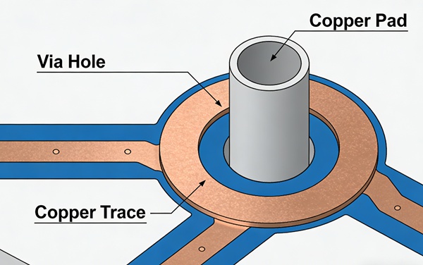
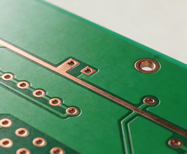
PCB Soldeermasker
Solder mask is a protective layer applied to the surface of printed circuit boards to prevent solder bridges and protect copper traces. Proper solder mask design is essential for reliable PCB assembly and manufacturing yield. This article explains key solder mask design guidelines including mask clearance, mask expansion, pad openings, and common layout mistakes. By following practical Design for Manufacturing (DFM) rules, engineers can improve assembly reliability, reduce solder defects, and ensure compatibility with standard PCB fabrication processes.