Productiefouten in PCB's zijn zelden willekeurig.
De meeste defecten ontstaan door ontwerpbeslissingen, materiaalbeperkingen of procesinstabiliteitlang voordat de eindinspectie plaatsvindt.
Terwijl inspectie veel zichtbare problemen kan opsporen, defectpreventie moet eerder in het productieproces plaatsvinden.
In dit artikel worden de meest voorkomende PCB fabricagefouten, hun hoofdoorzaken en praktische preventiestrategieën vanuit een productieperspectief uitgelegd.
Zie voor de basisprincipes van kwaliteit: Wat bepaalt de kwaliteit van PCB's?
Inhoudsopgave
Wat wordt beschouwd als een PCB fabricagefout?
Een PCB fabricagefout is elke afwijking die:
- Beïnvloedt de elektrische prestaties
- Compromitteert mechanische integriteit
- Vermindert de betrouwbaarheid op lange termijn
- In strijd is met IPC- of klantspecificaties
Defecten kunnen zijn zichtbaar, latentof progressiefdie alleen verschijnen na thermische of mechanische belasting.
Defecten binnenste laag
Veelvoorkomende defecten aan de binnenlaag
- Open circuits
- Kortsluiting
- Over-etsen of onder-etsen
- Foutieve registratie tussen lagen
Onderliggende oorzaken
- Onnauwkeurigheden in beeldvorming
- Variatie in etsproces
- Slechte uitlijning van de binnenlaag
Omdat de binnenlagen tijdens het lamineren worden verzegeld, zijn defecten in dit stadium onomkeerbaar.
Achtergrond van het proces: Uitleg over de fabricage van de binnenste laag
Geboorde defecten
Typische boorgebreken
- Gaten uit het midden
- Bramen en vlekken
- Kapotte boren
- Slechte kwaliteit van gatwand
Onderliggende oorzaken
- Overmatige hoogte-breedteverhouding
- Versleten gereedschap
- Verkeerde voeding en snelheid
- Ongeschikte boormethode
Defecten bij het boren hebben een directe invloed op de kwaliteit van het koperplateren en via de betrouwbaarheid.
Vergelijking van methoden:
PCB-boren vs. laserboren
Defecten aan het plateren
Veelvoorkomende galvanische problemen
- Dun koper in vias
- Leemtes of gaten
- Ruw of nodulair koper
- Slechte hechting
Onderliggende oorzaken
- Onjuiste voorbereiding van het oppervlak
- Inconsistente stroomdichtheid
- Chemische onbalans
- Vias met hoge hoogte-breedteverhouding
Plateerdefecten zijn een belangrijke oorzaak van intermitterende storingen en thermische cycli.
Procesdetail: Koperplateerproces bij PCB-productie
Etsdefecten
Typische etstefecten
- Overtrokken sporen
- Ondergeëtste koperen bruggen
- Variatie in lijndikte
- Trace nek omlaag
Onderliggende oorzaken
- Ongelijke koperdikte
- Agressieve etschemie
- Slechte procescompensatie
- Nauw aansluitende sporen
Naarmate de geometrie van de sporen fijner wordt, hebben etsfouten een steeds grotere invloed op de opbrengst en betrouwbaarheid.
Opbrengstgerichte analyse: PCB-etsproces en opbrengstcontrole
Defecten in laminering en delaminatie
Veelvoorkomende lamineerproblemen
- Delaminatie
- Zinderend
- Leemtes in hars
- Laagverschuiving
Onderliggende oorzaken
- Verkeerde lamineerdruk of -temperatuur
- Slechte prepreg selectie
- Vochtopname
- Ongebalanceerde stack-ups
Deze defecten komen vaak aan het licht tijdens de assemblage of thermische cycli in plaats van tijdens de eerste tests.
Materiële verwantschap: PCB-materiaal en -laagkosten
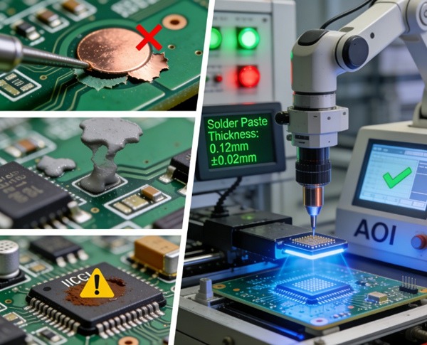
Defecten soldeermasker en oppervlakteafwerking
Typische defecten
- Verkeerde uitlijning soldeermasker
- Slechte hechting
- Speldenprikken
- Ongelijke dikte van oppervlakteafwerking
Onderliggende oorzaken
- Onjuiste voorbereiding van het oppervlak
- Onjuiste uithardingsomstandigheden
- Procesvervuiling
Deze defecten kunnen leiden tot soldeerbruggen, corrosie en een kortere houdbaarheid.
Elektrische testontsnappingen en latente defecten
Niet alle defecten worden ontdekt tijdens elektrische tests.
Latente defecten kunnen:
- Eerste tests doorstaan
- Storing na thermische belasting
- Verschijnen tijdens veldwerk
Veel voorkomende oorzaken zijn onder andere:
- Marginale plateerdikte
- Microscheurtjes in vias
- CAF-vorming
Ontwerpgerelateerde risico's op defecten
Sommige defecten zijn eerder het gevolg van ontwerpkeuzes dan van productiefouten.
Ontwerpfactoren met een hoog risico zijn onder andere:
- Uiterst fijne sporen en spatiëring
- Vias met hoge hoogte-breedteverhouding
- Ongebalanceerde koperdistributie
- Te krappe toleranties
Verbinding van ontwerpkwaliteit: Kostenfactoren PCB-ontwerp
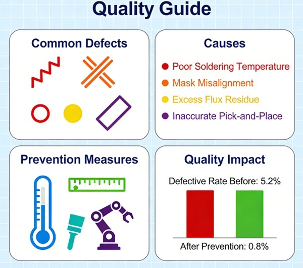
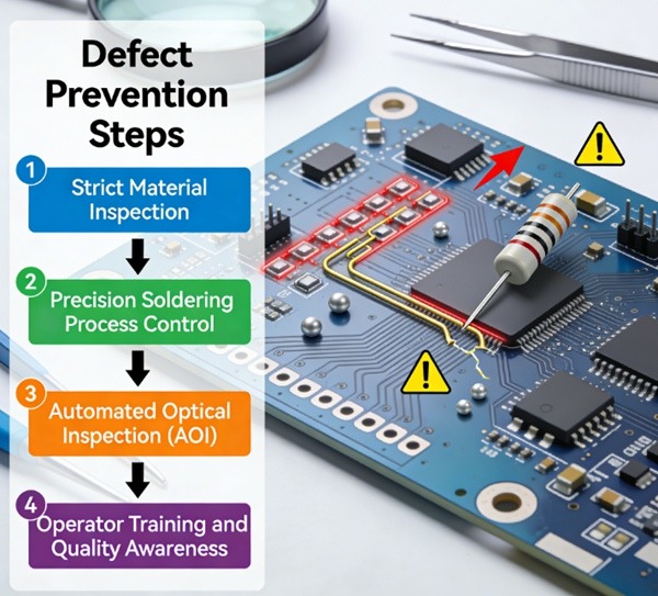
Hoe PCB-productiefouten voorkomen
Effectieve defectpreventie richt zich op processtabiliteitNiet alleen inspectie.
De belangrijkste preventiestrategieën zijn:
- Vroege DFM-beoordeling
- Conservatieve ontwerpmarges
- Gekwalificeerde materiaalselectie
- Bewaking van procesvermogen
- Analyse van opbrengstgegevens
Bij TOPFAST wordt defectpreventie gedreven door upstream procesbesturing en op gegevens gebaseerde feedbackwaardoor minder gebruik hoeft te worden gemaakt van end-of-line screening.
Preventie van defecten vs productiekosten
Het voorkomen van defecten verlaagt vaak de totale kosten.
Voordelen zijn onder andere:
- Hogere opbrengst
- Minder herwerk
- Minder vertragingen
- Lager risico op veldfouten
Balans tussen kosten en kwaliteit: Uitleg over de productiekosten van PCB's
Conclusie
Defecten in de productie van PCB's zijn zelden geïsoleerde incidenten.
Ze zijn het resultaat van interacties tussen ontwerp, materialen en procesbeheersing.
Door inzicht te krijgen in veelvoorkomende defecttypen en hun onderliggende oorzaken, kunnen technici en inkopers proactieve stappen ondernemen om defecten te voorkomen en de betrouwbaarheid op lange termijn te verbeteren.
Dit artikel vormt een kernpijler van de PCB-kwaliteit en -betrouwbaarheid cluster.
FAQ: PCB fabricagefouten
A: Defecten door etsen en platingproblemen komen het vaakst voor.
A: Nee. Inspectie spoort defecten op, maar voorkomt niet de hoofdoorzaken.
A: Thermische spanning tijdens assemblage kan latente defecten blootleggen die eerder zijn aangebracht.
A: Nee. Veel defecten ontstaan door ontwerp- of materiaalkeuzes.
A: Door middel van DFM-evaluatie en een conservatief ontwerp dat is afgestemd op de mogelijkheden van het proces.