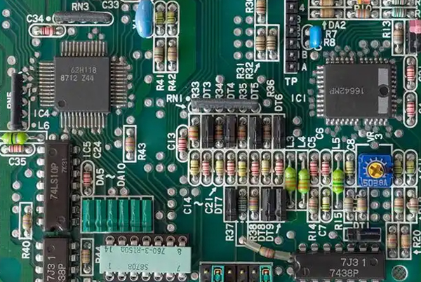
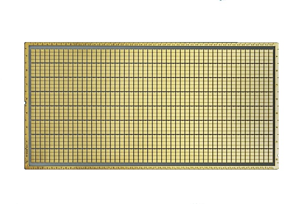
Demasiados componentes numa placa de circuito impresso causarão sobrecarga?
Quando há demasiados componentes numa placa de circuito impresso, isso pode levar a uma sobrecarga, o que pode causar efeitos adversos, como a degradação do desempenho elétrico e a redução da dissipação de calor. Assim, quando existem muitos componentes numa placa de circuito impressoComo podemos determinar se a placa de circuito impresso está sobrecarregada?
Índice
Métodos para determinar a sobrecarga de PCB
1. Ensaio dos parâmetros de corrente
- Utilizar uma pinça amperimétrica de alta precisão para medir a corrente de funcionamento dos circuitos críticos
- Comparar com os parâmetros de projeto:
- Os condutores convencionais de 1,5 mm² têm uma classificação de corrente segura de 16A (a uma temperatura ambiente de 30°C)
- A largura da linha de 100mil/1OZ de espessura de cobre tem uma classificação de corrente máxima de 4,5A (com base numa norma de aumento de temperatura de 10°C) - Critérios de determinação: Se a corrente medida for ≥80% do valor de projeto, é necessário um aviso
2.Análise das caraterísticas da subida de temperatura
- Ferramenta de teste:Termovisor de infravermelhos (resolução ≤ 0,1°C)
- Limiares de segurança:
- Material de isolamento em PVC: Temperatura do condutor ≤ 70°C
- Substrato FR-4:Aumento da temperatura local ≤ 20°C (relativamente à temperatura ambiente) - Indicadores anómalos:Descoloração/amaciamento da camada de isolamento, deformação da junta de soldadura
3.Verificação da capacidade de carga
- Fórmula de cálculo:I = Kx - P / (U - cosφ)
(Kx tomado como 0,7-0,8, cosφ recomendado como 0,85) - Exemplo de verificação:
Cálculo da corrente de carga resistiva 220V/3500W ≈ : 15,9A
Requer um fio de 2,5 mm² correspondente (margem de conceção de 20%)
4.Diagnóstico da condição física
- Caraterísticas típicas de falha:
- Descolamento da folha de cobre (tensão de corte superior ao limite)
- Marcas de carbonização (alta temperatura localizada > 300°C)
- Funcionamento anormal dos dispositivos de proteção (≥3 disparos em 24 horas)
5.Verificação da especificação do projeto
Tabela de correspondência de parâmetros-chave:
| Necessidade atual | Requisito de espessura do cobre | Largura mínima da linha | Medidas complementares |
|---|---|---|---|
| <5A | 1OZ | 20mil | Encaminhamento de uma face |
| 5-20A | 2OZ | 80mil | Adicionar janelas |
| >100A | 4OZ | 15 mm | Assistência a barramentos de cobre |
Dar prioridade ao rastreio rápido através da medição da corrente + monitorização da temperatura, combinada com o cálculo da carga e a verificação cruzada da inspeção física. Para placas de circuito impresso de alta potência, selecionar rigorosamente a largura da linha e a espessura do cobre de acordo com a tabela de capacidade de transporte de corrente na fase inicial do projeto e reservar uma margem de dissipação de calor. Que consequências terá a sobrecarga na placa de circuito impresso?
Efeitos da sobrecarga nos PCB
1. Mecanismo de destruição tripla do desempenho elétrico
- Efeito de instabilidade de impedância
Aumento significativo da resistência do fio: ΔR = ρ - L - (1/S₁ – 1/S₂) (S é a alteração da área da secção transversal)
Caso típico: A sobrecarga das linhas de alimentação provoca uma flutuação de ±15% na tensão de alimentação da MCU, accionando a reinicialização do sistema (dados de medição reais) - Colapso da integridade do sinal
Métricas de degradação do sinal de alta velocidade:
Fecho do diagrama ocular > 30%
Skew de atraso ≥ 50 ps
Relação de ruído cruzado > -12 dB - Radiação 3EMI que excede as normas
Os níveis de pico de EMI em linhas sobrecarregadas aumentam 20-35 dBμV/m
Exemplo de degradação da relação sinal/ruído em circuitos sensíveis:
A taxa de erro de amostragem do ADC de áudio aumenta de 0,1% para 3,2%
2.Espectro termodinâmico de falhas
- Limiares de danos materiais Tipo de material Temperatura crítica Modo de falha Substrato FR-4 130°C Delaminação e fissuração Folha de cobre de 1 oz 260°C Fusão e deformação Solda de chumbo-estanho 183°C Migração líquida Tinta da máscara de solda 70°C Carbonização e descamação
- Cadeia típica de falhas térmicas
Sobrecorrente → Aumento da temperatura local > 85°C → Fluência da junta de soldadura → Aumento da resistência de contacto → Fuga térmica (ciclo de feedback positivo)
3.Matriz de risco a nível do sistema
- Distribuição da probabilidade de falha
Módulo de potência: 68%
Interface de alimentação: 22%
Linhas de sinal: 10% - Modelo de dano secundário
Raio de influência da radiação térmica: R = 3,5 - √P (P é a potência de geração de calor, unidade: W)
Caso:Uma fonte de calor de 10W provoca um desvio da capacidade de ±15% num raio de 3cm do MLCC
Solução do sistema de sobrecarga de PCB (sistema de otimização de quatro dimensões)
1. Solução de melhoria do desempenho elétrico
- Capacidade de carga atual Melhoria
- Otimização da camada de cobre: Cobre com 4OZ de espessura + cablagem de dupla face com 15 mm de largura (solução de nível 100A)
- Processos melhorados:
Estanhagem de abertura de janelas nos condutores (melhoria de 40% da capacidade de transporte de corrente)
Partilha de corrente auxiliar de barramento de cobre (caso de aplicação de 200A de nível industrial)
- Tecnologia de controlo de impedância
- Camada de potência com conceção de plano de cobre completo (impedância < 5mΩ)
- Matriz via matriz (12mil via grupo partilhando 20A de corrente)
2.Solução inteligente de gestão térmica
- Conceção da estrutura de dissipação de calor
- Configuração de componentes de alto calor (>5W):
Conjunto de orifícios de dissipação de calor na parte inferior (Φ0,3 mm×50 orifícios)
Disposição dos bordos da placa + dissipador de calor em liga de alumínio (queda de temperatura de 60%)
- Especificações da disposição térmica
- Espaçamento entre componentes de sensibilidade térmica ≥8mm
- Distribuição uniforme das fontes de calor (controlo da diferença de temperatura <15°C)
3.Estratégia de disposição de alta densidade
- Conceção da integridade do sinal
- Isolamento da camada digital/analógica (blindagem intermédia da camada GND)
- Sinais de alta velocidade:
Controlo de comprimento igual (±50 mil)
Disposição simétrica dos componentes RF (redução de ruído de 12 dB para módulos 5G)
- Solução de isolamento de alta tensão
- Áreas >50V:
Espaçamento de segurança de 15 mm
Isolamento da ranhura com isolamento de 2 mm
4.Soluções de processo avançadas
- Processo de laminação especial
- Estrutura de camada de cobre em sanduíche (camada de cobre incorporada de 1,5 mm)
- Aplicação de material de placa de alta frequência (Rogers 4350B@1GHz+)
- Sistema de verificação
- Simulação térmica (ΔT < 15°C/cm)
- Ensaio de sinal (flutuação da impedância do TDR ≤ 10%)
- Normas DFM (largura/espaçamento da linha ≥ 4 mil)
| Fase de otimização | Principais indicadores técnicos |
|---|---|
| 1. Fundamentos da capacidade atual | Espessura do cobre ≥4OZ + Largura do traço ≥15mm |
| 2. Gestão térmica | Redução da temperatura dos componentes principais ≥30% |
| 3. Otimização do sinal | Redução de diafonia 12dB |
| 4. Atualização do processo | Melhoria da taxa de rendimento em 27% |
Nota: Após a aplicação desta solução a um módulo de estação de base 5G, foram obtidos os seguintes resultados:
- Capacidade de transporte de corrente contínua aumentada em 300%
- A taxa de falha térmica diminuiu 82%
- A taxa de conformidade da integridade do sinal atingiu 100%
Para evitar a sobrecarga de PCB, que medidas devem ser tomadas? A prevenção da sobrecarga de PCB requer um controlo colaborativo ao longo de todo o processo de conceção, fabrico e teste.
Plano de proteção contra sobrecarga de PCB
1. Estratégia de proteção na fase de conceção
- Conceção exacta da capacidade de carga atual
- Norma de cálculo da capacidade de carga atual:
matemática
I_{max} = K \cdot \Delta T^{0.44} \cdot W^{0.725}
(K=0,048, ΔT é o aumento de temperatura admissível, W é a largura da linha em mils) - Esquemas de configuração típicos:
- Aplicações convencionais: 2OZ de espessura de cobre + 100mil de largura de linha (classe 10A)
- Esquemas de corrente elevada:4OZ de espessura de cobre + traços de 15mm de dupla face + barramentos de cobre (classe 100A)
- Conceção da integridade da energia
- Matriz de condensadores de desacoplamento:
- Banda de alta frequência: 0402 Condensador cerâmico de 10nF (ESL < 0,5nH)
- Banda de média frequência: condensador 0603 100nF
- Banda de baixa frequência: condensador de tântalo 1206 10μF
- Gestão térmica melhorada
- Especificações da matriz de orifícios de dissipação de calor:
- Diâmetro do furo: Φ0.3mm
- Distância central:0,8 mm
- Disposição em favo de mel (melhoria de 35% na eficiência da dissipação de calor)
2.Processos de fabrico avançados
- Tecnologias de processamento especial
- Processo de elevada capacidade de transporte de corrente:
- Enchimento de cobre VIPPO (redução de 40% da resistência de contacto)
- Espessura selectiva de cobre (espessamento de 4OZ em áreas locais)
- Sistema de proteção
- Parâmetros do processo de revestimento de três provas:
| Tipo de revestimento | Espessura | Temp. Resistência | Teste de pulverização de sal | Caraterísticas principais |
|---|---|---|---|---|
| Silicone | 0,1 mm | 200°C | 1000 horas | Elevada flexibilidade, excelente resistência à humidade |
| Poliuretano | 0,15 mm | 130°C | 500 horas | Resistência superior à abrasão, boa proteção química |
3.Sistema de teste e monitorização
- Normas de ensaio de produção
- Itens do teste TIC:
- Teste de impedância (tolerância de ±5%)
- Resistência de isolamento (≥100MΩ)
- Teste de tensão de resistência (500V DC/60s)
- Sistema de monitorização inteligente
- Parâmetros de monitorização em tempo real:
- Densidade de corrente (≤4A/mm²)
- Temperatura do ponto de acesso (≤85℃)
- Espectro de vibração (<5g RMS)
4.Principais especificações de projeto
| Classificação atual | Espessura do cobre | Mín. Largura do traço | Aumento da temperatura máxima | Recomendações de conceção |
|---|---|---|---|---|
| ≤5A | 1 oz (35μm) | 50 mil (1,27 mm) | ≤10°C | Encaminhamento de camada única |
| 20A | 2 oz (70μm) | 3mm | ≤15°C | Via térmica |
| 100A+ | 4 oz (140μm) | 15 mm | ≤20°C | Barramento de cobre com arrefecimento líquido |
5.Soluções de elevada fiabilidade
- Proteção de nível militar
- Conceção de laminado simétrico (≤5% de desvio de impedância)
- Embalagem cheia de nitrogénio (teor de oxigénio <100ppm)
- Sistema de aviso de avaria
- Mecanismo de aviso de três níveis:
Nível 1: Alarme sonoro e visual quando a temperatura ultrapassa os 85°C
Nível 2: Redução automática da frequência quando a corrente excede o limite
Nível 3: Proteção por fusível (tempo de ação < 50 ms)
Resumo
Os problemas de sobrecarga de PCB envolvem a degradação do desempenho elétrico, falhas térmicas e riscos de estabilidade do sistema, e devem ser controlados ao longo de todo o processo de conceção, fabrico e teste. Ao utilizar cálculos precisos da capacidade de transporte de corrente (por exemplo, espessura de cobre de 4 oz + largura de traço de 15 mm suportando 100 A), design térmico avançado (matrizes de orifícios de dissipação de calor em favo de mel reduzindo o aumento de temperatura em 35%), controlo rigoroso do processo (enchimento de cobre VIPPO reduzindo a resistência em 40%) e monitorização inteligente (alertas de corrente/temperatura em tempo real), a fiabilidade da PCB pode ser significativamente melhorada.


Publicações relacionadas