Aşındırma işlemi kaplanmış bakırı hassas devre desenlerine dönüştürür.
Yüzeyde basit görünse de, aşındırma en zor işlerden biridir. verime en duyarlı adımlar PCB üretiminde.
Bir üreticinin bakış açısından, zayıf dağlama kontrolü şunlara yol açar:
- Çizgi genişliği değişimi
- Şortlar ve açıklıklar
- Düşük verim
- Daha yüksek üretim maliyeti
Bu makalede PCB aşındırmanın nasıl çalıştığı, aşındırma kalitesini nelerin etkilediği ve aşağıdaki gibi üreticilerin nasıl çalıştığı açıklanmaktadır TOPFAST tutarlı, uygun maliyetli PCB üretimi sağlamak için verimi kontrol edin.
İçindekiler
PCB Aşındırma Nedir?
PCB aşındırma kimyasal bir işlemdir istenmeyen bakırı giderir Karttan sadece tasarlanan devre modelini bırakarak.
Aşındırma işlemi uygulanır:
- İç katmanlar
- Dış katmanlar
Hedefe ulaşmak için doğru iz genişliği, aralığı ve geometrisi tasarım özelliklerine göre.
PCB Aşındırma İşlemlerinin Türleri
İç Katman Aşındırma
İç katman aşınması meydana gelir:
- Laminasyondan önce
- İnce bakır folyo üzerine
Oldukça hassastır çünkü:
- Laminasyondan sonra kusurlar onarılamaz
- İç katman verimi tüm PCB yığınını etkiler
Dış Katman Aşındırma
Dış katman aşınması meydana gelir:
- Bakır kaplamadan sonra
- Daha kalın bakır katmanlarda
Dış katman aşındırması hesaba katılmalıdır:
- Kaplama bakır kalınlığı
- Panel genelinde tekdüzelik
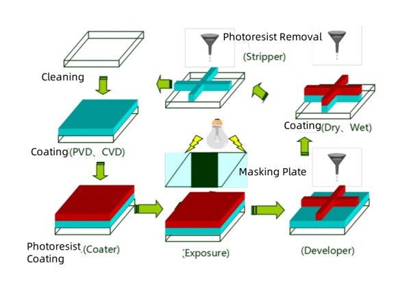
Adım Adım PCB Aşındırma Süreci
Adım 1 - Direnç Kalıbı Hazırlama
Bir direnç katmanı, aşındırmadan sonra kalması gereken bakır alanları korur.
Bu aşamadaki desen doğruluğu nihai iz geometrisini belirler.
Adım 2 - Kimyasal Aşındırma
Kimyasal çözeltiler açıkta kalan bakırı seçici olarak uzaklaştırır.
Temel süreç değişkenleri:
- Etchant konsantrasyonu
- Sıcaklık
- Püskürtme basıncı
- Aşındırma süresi
Bu değişkenlerin kontrol edilmesi istikrarlı sonuçlar için gereklidir.
Adım 3 - Direnç Sıyırma
Aşındırma işleminden sonra, kalan direnç kaldırılır ve bitmiş bakır izleri ortaya çıkar.
Yaygın Aşındırma Hataları ve Etkileri
Üstten Gravür
Sebepler:
- Aşırı aşındırma süresi
- Agresif kimya
Sonuçlar:
- Azaltılmış iz genişliği
- Artan empedans
- Potansiyel açılır
Gravür Altı
Sebepler:
- Yetersiz aşındırma süresi
- Zayıf etchant aktivitesi
Sonuçlar:
- Artık bakır
- İzler arasındaki şortlar
Alttan Kesme
Etchant, direnç altındaki bakırı yanlara doğru kaldırarak iz genişliğini azaltır.
Alttan kesme daha şiddetli hale gelir:
- Daha kalın bakır
- Daha ince iz tasarımları
PCB Üretiminde Verim Nedir?
Verim şu anlama gelir spesifikasyonları karşılayan panoların yüzdesi üretimden sonra.
Yüksek verim demektir:
- Birim başına daha düşük maliyet
- İstikrarlı kalite
- Öngörülebilir teslimat
Düşük verim yol açar:
- Hurda
- Rework
- Daha yüksek toplam maliyet
Aşındırma Üretim Verimini Nasıl Etkiler?
Aşındırma verimi doğrudan etkiler çünkü:
- İz kusurları elektrik arızasına neden olur
- İç katman kusurları paneller arasında çoğalıyor
- Küçük farklılıklar yüksek yoğunluklu tasarımları etkiler
Bir üreticinin bakış açısından, aşındırma en yüksek kaldıraç noktaları verim iyileştirmesi için.
Dağlama Verimini Etkileyen Tasarım Faktörleri
Tasarımlar yapıldığında verim artar:
- Gereksiz ince izlerden kaçının
- Tutarlı çizgi genişliğini koruyun
- Bakır dağıtımını dengeleyin
- Üreticinin önerdiği minimum aralığı kullanın
DFM inceleme genellikle aşındırma ile ilgili riskleri erken ortaya çıkarır.
Üreticiler Aşındırma Verimini Nasıl Kontrol Ediyor?
Süreç İzleme
Anahtar kontroller şunları içerir:
- Sürekli kimya analizi
- Ekipman kalibrasyonu
- Gerçek zamanlı çizgi genişliği ölçümü
Panel Düzeyinde Optimizasyon
Üreticiler optimize eder:
- Panel düzeni
- Bakır dengesi
- Panel boyunca aşındırma homojenliği
Denetim ve Geri Bildirim
AOI ve elektriksel testler için geri bildirim sağlar:
- Aşındırma parametrelerini ayarlayın
- Süreç istikrarını iyileştirin
TOPFAST'ta verim verileri, aşındırma süreçlerini iyileştirmek ve sorunların tekrarlanmasını önlemek için aktif olarak kullanılır.
Aşındırma ve Verim Kaybının Maliyete Etkisi
Düşük verim nedeniyle maliyet artar:
- Hurda malzemeler
- Ek işçilik
- Üretim gecikmeleri
Aşındırma veriminin iyileştirilmesi genellikle aşağıdakilerden daha etkilidir kesme malzemesi maliyeti PCB fiyatını düşürürken.
Üretici Perspektifi: TOPFAST'ın Verim Odaklı Aşındırma Stratejisi
TOPFAST aşındırma verimini kontrol eder:
- Standartlaştırılmış süreç pencereleri
- Muhafazakar tasarım önerileri
- Erken DFM geri bildirimi
- Sürekli verim izleme
Odak noktası tutarlı kalite ve ölçeklenebilir üretimSadece minimum toleransları karşılamak değil.
Sonuç
PCB aşındırma, aldatıcı bir şekilde basit bir işlemdir. verim, maliyet ve güvenilirlik üzerinde büyük etki.
Aşındırmanın nasıl çalıştığını ve verimi nelerin etkilediğini anlayarak, tasarımcılar ve alıcılar daha akıllıca kararlar verebilirler:
- Üretim riskini azaltın
- Daha düşük toplam maliyet
- Ürün güvenilirliğini artırın
Verim odaklı üretim yaklaşımı ile, TOPFAST ölçekte güvenilir PCB üretimini destekleyen istikrarlı aşındırma kalitesi sağlar.
İlgili Okuma
PCB Üretim Süreci PCB Üretim Süreci
Aşındırma Verim Kontrolü SSS
C: PCB aşındırma, devre desenleri oluşturmak için istenmeyen bakırı kaldıran kimyasal bir işlemdir.
C: Aşırı aşındırma, aşırı aşındırma süresi veya aşırı agresif kimyasal çözeltilerden kaynaklanır.
C: Kötü aşındırma kontrolü iz hatalarına yol açarak verimi düşürür ve maliyeti artırır.
C: Evet. Makul iz genişliklerine ve aralıklara sahip tasarımlar aşındırma verimini önemli ölçüde artırır.
C: TOPFAST, istikrarlı aşındırma verimini korumak için standartlaştırılmış süreçler, gerçek zamanlı izleme ve DFM geri bildirimi kullanır.