0.1nh Smd Inductor
A chip inductor is a common electronic component used in circuits for functions such as filtering, regulation, and coupling. It is usually made from a solenoid coil wound around a chip of insulating material. This solenoid can be cylindrical, square, or other shapes, depending on the specific design needs.
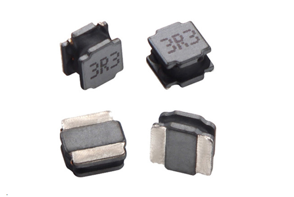
Table of Contents
What is a 0.1nh Chip Inductor?
A chip inductor (SMD inductor) is a surface-mount passive component that stores electromagnetic energy and provides filtering via a coiled structure. Among these, the 0.1nH (0.1 nanohenry) inductor represents an extremely low inductance value, designed for ultra-high-frequency (UHF) circuits where minimal inductance is critical.
1.Key Characteristics of 0.1nH Chip Inductors
- Ultra-low inductance: 0.1nH (1×10¹⁰ H) is a tiny inductance value, typically achieved using very short traces or micro-coils, where parasitic effects (e.g., distributed capacitance) become significant.
- High-frequency applications: Primarily used in millimeter-wave (mmWave), 5G communications, RF front-ends (e.g., antenna matching), and high-speed digital circuits (e.g., PCIe/USB signal integrity optimization).
- Simplified structure: Some 0.1nH inductors may be implemented as PCB traces (microstrip lines) or ultra-compact SMD packages (e.g., 0201/01005).
2.Fundamentals of General Chip Inductors
- Standard packages: 0402, 0603, 0805, etc., though 0.1nH variants may require even smaller designs.
- Core functions: Filtering (EMI suppression), energy buffering (DC-DC converters), and impedance matching (RF circuits).
- Critical parameters: Beyond inductance, consider self-resonant frequency (SRF), rated current (often in mA range), and Q-factor (high-frequency loss).
3.Selection Guidelines for 0.1nH Inductors
- High-frequency performance: Ensure the SRF is well above the operating frequency (e.g., >100 GHz for 77 GHz automotive radar).
- Parasitic effects: Low-value inductors are sensitive to pad layout and trace routing—verify via simulation or testing.
- Alternative solutions: In some cases, a short wire jumper may suffice, but consistency and thermal drift must be evaluated.
4.Typical Applications
- RF modules: Fine-tuning impedance at power amplifier (PA) outputs.
- High-speed digital circuits: Mitigating reflections in GHz-range signals (stub compensation).
- Microwave systems: Matching networks for waveguide-to-chip transitions.
5.Comparison with Conventional Inductors
| Parameter | 0.1nH Chip Inductor | Standard Chip Inductor (e.g., 1µH) |
|---|---|---|
| Frequency Range | >10 GHz | <1 GHz |
| Primary Use | Signal integrity | Power filtering |
| Structure | Possibly coreless | Ferrite/ceramic core |
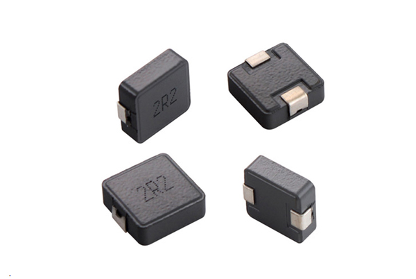
Basic Structure and Types of Chip Inductors
1. Core Structural Components
Surface mount chip inductors primarily consist of three key elements:
- Coil
- Material: High-purity copper wire or alloy conductors (e.g., silver-palladium), with some high-frequency variants using gold plating.
- Process: Precision winding or photolithography (for thin-film types), affecting DC resistance (DCR) and frequency response.
- Magnetic Core
- Common Materials: Ferrite (low-frequency, high-inductance), nickel-zinc ferrite (high-frequency, low-loss), or amorphous alloys (high-current applications).
- Function: Enhances permeability to increase inductance but may introduce saturation issues (check rated current).
- Encapsulation/Housing
- Protection: Ceramic or resin casing provides mechanical stability and environmental resistance (moisture/oxidation protection).
- Terminals: Tin- or silver-plated electrodes ensure soldering reliability.
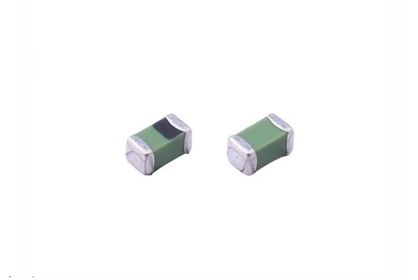
2. Main Types and Characteristics Comparison
Based on construction methods, chip inductors are categorized into four types:
| Type | Wire-Wound | Multilayer | Thin-Film | Braided |
|---|---|---|---|---|
| Structure | Copper wire on the core | Laminated magnetic layers | Photolithographed traces | Interwoven metal fibers |
| Inductance | Wide (nH–mH) | Small (nH–μH) | Ultra-low (0.1nH–100nH) | Medium-high (μH-range) |
| Tolerance | ±2%–±5% | ±5%–±10% | ±0.1nH (high-precision) | ±10%–±20% |
| Q Factor | High (50–100) | Moderate (20–50) | Very high (>100, RF-fit) | Low (<20, power-rated) |
| Advantages | High accuracy, low loss | Compact, closed magnetic path | Ultra-high-frequency, miniaturized | High current, anti-saturation |
| Limitations | Size constraints | Narrow inductance range | Minimal inductance | Bulky, poor high-freq. performance |
| Applications | Power filtering, low-frequency. resonance | Smartphones, IoT devices | 5G/mmWave, RF ICs | High-current DC-DC conversion |
Working Principle and Key Functions of 0.1nH Chip Inductors
1. Working Principle (Based on Faraday’s Law of Electromagnetic Induction)
- Electromagnetic Energy Conversion
- When current flows through the inductor coil, it generates a circular magnetic field, with field strength proportional to the current (Ampère’s Circuital Law).
- When current changes (e.g., high-frequency signals), the varying magnetic field induces a back EMF (Lenz’s Law), resisting sudden current fluctuations.
- Frequency Characteristics
- Blocks AC, Passes DC: Near-zero impedance for DC (0Hz), while AC impedance increases with frequency (XL=2πfL).
- Unique Traits of 0.1nH Inductors:
- Extremely low inductance results in minimal impedance (e.g., only 0.63Ω at 1GHz), making it ideal for ultra-high-frequency signal paths (e.g., mmWave bands).
- Parasitic capacitance (typically 0.1–0.5pF) may cause self-resonance—selection must consider SRF (Self-Resonant Frequency).
2. Four Core Functions of 0.1nH Chip Inductors
| Function | Mechanism | Typical Applications |
|---|---|---|
| High-Freq. Filtering | Forms LC filters with capacitors to absorb noise (e.g., power ripple, RF interference). | 5G base station PA decoupling, CPU power circuits |
| Energy Buffering | Temporarily stores energy in switching circuits (e.g., DC-DC converters) to reduce voltage fluctuations from current spikes. | Buck/Boost converter high-frequency nodes |
| Impedance Matching | Adjusts RF path impedance (e.g., antenna interfaces) to minimize signal reflection and improve transmission efficiency. | mmWave radar RF frontends, Wi-Fi 6E antenna design |
| EMI Suppression | Cancels high-frequency radiated noise via magnetic flux cancellation, reducing electromagnetic leakage with shielding. | High-speed SerDes interfaces, satellite comms modules |
3. Unique Advantages of 0.1nH Inductors
- Ultra-High-Frequency Suitability
- Operates up to 30GHz+ (e.g., Ka-band satellite comms), where traditional wire-wound inductors fail due to parasitic effects.
- Miniaturized Integration
- 01005 package (0.4×0.2mm) enables high-density PCB embedding, ideal for SiP (System-in-Package) designs.
- Low Insertion Loss
- Compared to higher-inductance parts, it introduces less loss in mmWave bands (<0.1dB@60GHz).
Professional SMD Inductor Soldering Guide
I. Pre-Soldering Preparation
- Tools & Materials Checklist
- Essential tools: Temperature-controlled soldering station (280-320℃ recommended), lead-free solder wire (0.3-0.5mm diameter), ESD-safe precision tweezers, adjustable hot air gun
- Auxiliary equipment: Soldering microscope (10-20x magnification), no-clean flux, desoldering braid
- Safety: ESD wrist strap, fume extraction system
- PCB Pre-Treatment
- Clean pads with alcohol wipes to remove oxidation
- Verify pad dimensions match inductor terminals (0.2mm extension recommended)
- Confirm polarity markings (critical for power inductors)
II. Standard Soldering Procedure (Hand Soldering)
| Step | Key Operations | Technical Parameters |
|---|---|---|
| 1. Placement | Use a vacuum pen or ESD tweezers for precision alignment | Position tolerance ≤0.1mm |
| 2. Preheating | Preheat PCB to 80-100℃ with hot air gun (5cm distance) | Airflow level 2-3, 200℃ |
| 3. Temporary Fixation | Tack solder one corner terminal first | Soldering iron at 300±10℃ |
| 4. Full Soldering | Apply the drag soldering technique for the remaining terminals | Contact time <3s per joint |
| 5. Inspection | Examine joint morphology under a microscope | Smooth concave fillet required |
III. Critical Considerations
- Temperature Management
- Ferrite core inductors: Max 300℃
- Thin film inductors: Use low-temp solder (138℃ melting point)
- Maximum continuous heating: 5 seconds
- Special Type Handling
- High-current inductors: Additional solder paste on the bottom pad
- RF inductors: Avoid silver-containing solder (affects Q-factor)
- Micro inductors (01005): Recommended reflow process
- Troubleshooting
- Bridging: Remove with desoldering braid
- Cold joints: Reflow with added flux
- Component shifting: Use adhesive dispensing
IV. Post-Soldering Verification
- Electrical Tests:
- LCR meter measurement (deviation <±5%)
- DCR compliance check
- Mechanical Tests:
- Push-pull test (2.5 kgf standard)
- X-ray inspection for internal integrity
- Environmental Tests:
- Thermal cycling (-40℃~125℃)
- Vibration testing (10- 500Hz sweep)
V. Process Optimization
- Mass Production:
- Recommended reflow profile optimization
- Peak temperature by size:
- 0603: 235-245℃
- 0402: 230-240℃
- Rework Guidelines:
- Use dedicated heating fixtures
- Strictly control the reheat duration
SMD inductors for the field
1.power supply circuit: such as a switching power supply, DC-DC converter.
2.communication equipment: such as cell phones, wireless communication modules.
3.high-frequency circuits: such as radio frequency (RF) circuits, radar.
4.consumer electronics: such as notebook computers, tablet computers.


Related Posts