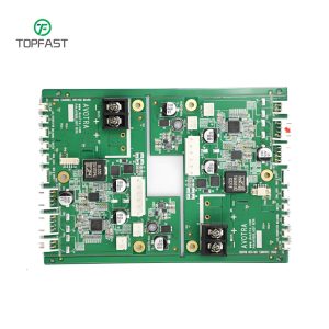
In the Surface Mount Technology (SMT) production process, the quality of the solder paste printing stage directly determines the final product’s soldering reliability. 3D-SPI (Three-Dimensional Solder Paste Inspection), as a crucial quality inspection step after printing, effectively intercepts printing defects through precise three-dimensional measurement technology, becoming the “quality gatekeeper” that enhances the yield rate of SMT production lines.
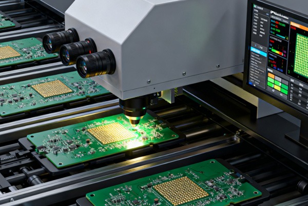
Table of Contents
What is SPI Solder Paste Inspection?
SPI Solder Paste Inspection is a specialized testing technology that uses optical inspection equipment to measure three-dimensional parameters of solder paste printed on PCBs, comparing them against preset standards to determine printing quality.
Position of SPI in the SMT Production Process:
Solder Paste Printing → 3D-SPI Inspection → Component Placement → Reflow Soldering → Final InspectionCore Value: Identifying printing issues before soldering, preventing defects from flowing into subsequent processes, and reducing batch rework losses.
Detailed Working Principle of 3D-SPI
Optical Imaging System
- Projection Module: Laser lines, structured light, or multi-frequency gratings
- Acquisition Module: High-resolution multi-angle cameras
- Inspection Principle: Structured light triangulation method
3D Reconstruction Process
- Grating Projection → 2. Distorted Image Acquisition → 3. 3D Data Calculation → 4. Parameter Analysis
Comparison Between 2D-SPI and 3D-SPI Technologies
| Dimension | Measurement Parameters | Accuracy | Application Scenarios |
|---|---|---|---|
| 2D-SPI | Area, Position | Lower | Simple PCB boards |
| 3D-SPI | Volume, Height, Area, Shape | High Precision | High-density, miniaturized components |
Core Functions of SPI in Quality Control
1. Defect Interception and Prevention
- Main Types of Detected Defects:
- Insufficient Solder (Low Volume)
- Excessive Solder (Over Volume)
- Misalignment (Position Deviation)
- Bridging (Connection Between Adjacent Pads)
- Shape Abnormalities (Peaking, Depression)
2. Process Optimization and Closed-Loop Control
The analysis of inspection data provides feedback to optimize solder paste printing parameters:
- Squeegee pressure and speed optimization
- Stencil aperture size verification
- Printing machine accuracy calibration
3. Data-Driven Decision Making
- Real-time Monitoring: Immediate feedback of quality data during production
- Statistical Analysis: Support for SPC (Statistical Process Control)
- Quality Traceability: Complete inspection history recorded for each PCB
Analysis of 3D-SPI Inspection Process
Complete Inspection Cycle

Detailed Key Steps
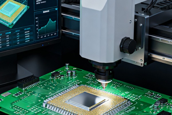
Step 1: PCB Positioning and Pre-processing
- Precise positioning using Mark points (accuracy ≤ ±0.01mm)
- Surface cleaning and dust removal to ensure inspection accuracy
Step 2: 3D Scanning and Imaging
- Structured light projection, multi-angle image acquisition
- Typical single board inspection time ≤ 2 seconds, matching production line cycle time
Step 3: Data Analysis and Judgment
- Core Inspection Parameters and Standards:
| Parameter | Inspection Content | Typical Tolerance Standard |
|---|---|---|
| Volume | Solder Paste Capacity | ±15% of standard value |
| Height | Solder Paste Thickness | According to process requirements |
| Area | Coverage Area | ≥85% of pad area |
| Offset | Position Accuracy | ≤0.1mm |
Step 4: Result Feedback and Processing
- Qualified products: Automatically flow to the placement process
- Non-conforming products: Audio-visual alarm, visual display of defect locations
- Rework guidance: Provides specific repair solutions (solder supplement, wiping, etc.)
Step 5: Data Management and Analysis
- Inspection data uploaded to the MES system
- Quality report generation, identifying trend issues
- Providing data support for continuous improvement
Development Trends in Advanced SPI Technology
Intelligent Closed-Loop Control System
Modern SPI systems not only detect defects but also enable automatic adjustment of process parameters:
- Reverse Closed Loop: Feeds inspection data back to the solder paste printer for automatic correction of printing parameters
- Forward Closed Loop: Transfers actual solder paste positions to the placement machine to adjust component placement positions
Integrated Quality Platform
Such as Viscom’s Quality Uplink function, enabling centralized analysis of data from all inspection systems on the production line, supporting real-time process optimization.
Economic Benefits of SPI Implementation
Return on Investment Analysis:
- Defect detection rate increased to over 99%
- Reduction in batch rework caused by printing issues
- Decrease in material waste and labor costs
- Improved final product reliability, reduced after-sales maintenance
Application Scenarios and Selection Recommendations
Suitable Industries
- Consumer Electronics (Smartphones, Tablets)
- Automotive Electronics (Safety-critical systems)
- Medical Equipment (High reliability requirements)
- Industrial Control (Long-term stable operation)
Technical Selection Considerations
- PCB board size and complexity
- Production cycle time requirements
- Inspection accuracy needs
- System integration capabilities
- Budget and return on investment expectations
Conclusion
3D-SPI solder paste inspection technology has become an indispensable quality control link in modern SMT production. Through precise three-dimensional measurement, real-time defect interception, and process parameter optimization, SPI not only improves production yield and efficiency but also provides technical assurance for the reliable manufacturing of high-density, miniaturized electronic products. With continuous improvements in intelligence and integration levels, SPI will play an even more critical role in electronic manufacturing quality control.