Since its introduction in the 1980s, the Ball Grid Array (BGA) package has rapidly become the preferred packaging form for high-density integrated circuits due to its high pin density, excellent electrical and thermal performance, and reliability. Evolving from early standard BGAs with 1.27mm pitch to today’s wafer-level chip scale packages (WLCSP) with 0.4mm or even finer pitch, BGA technology continues to drive the miniaturization and high performance of electronic devices.
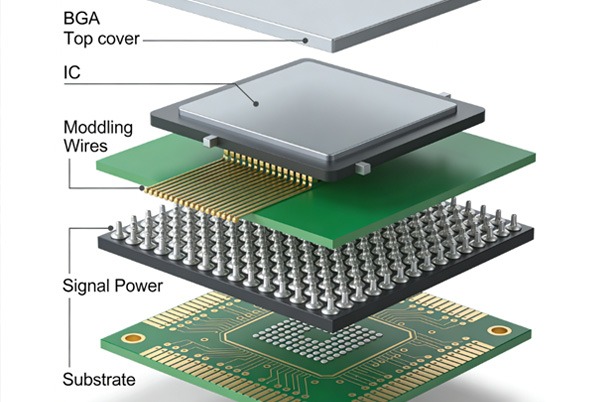
Table of Contents
Current Design Challenges
- Soaring Pin Density: Modern processors often integrate 1000+ pins, with pitches compressed below 0.5mm.
- Signal Integrity Demands: High-speed interfaces (PCIe, DDR) impose stringent requirements for impedance control and crosstalk suppression.
- Thermal Management Complexity: Increased power density exacerbates risks of local overheating.
- Manufacturing Process Limits: Traditional PCB processes face challenges like microvias, via filling, and alignment accuracy.
BGA Pad Layout: From Theoretical Calculation to Engineering Implementation
2.1 Scientific Calculation of Pad Size
The relationship between pad diameter (d) and solder ball diameter (dball) is not a fixed ratio but should be based on the solder volume model:

Where:
- (k): Wetting coefficient (typically 0.8-0.9)
- (process): Manufacturing tolerance compensation (typically 0.05-0.1mm)
TOPFAST Practical Experience: For a 0.5mm pitch BGA, we recommend:
- Pad diameter of 0.25-0.28mm for a solder ball diameter of 0.3mm.
- Using NSMD (Non-Solder Mask Defined) design, with solder mask opening 0.05-0.1mm larger than the pad.
- Adding silkscreen markings in the A1 identifier area for easier assembly alignment.
2.2 Pitch Design and Escape Channel Planning
The escape routing capability determines the feasibility of the BGA design. The number of routing channels (Nescape) can be estimated by:

Where:
- (p): Ball pitch
- (w): Trace width
- (s): Trace spacing
Multi-Layer Allocation Strategy:
| BGA Rows | Minimum Signal Layers | Recommended Layer Allocation |
|---|---|---|
| ≤5 rows | 2 layers | Top layer + Inner layer 1 |
| 6-8 rows | 3-4 layers | Top layer + 2-3 inner layers |
| ≥9 rows | 5+ layers | Requires HDI or buried vias |
Thermal Relief Pads: Fine-Tuned Balance in Thermal Management
3.1 Thermodynamic Principles and Parameter Optimization
Thermal relief pads regulate heat flow by controlling the cross-sectional area of the copper connection. Their thermal resistance model is:
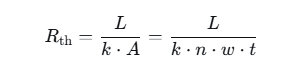
Where:
- (n): Number of spokes (typically 2-4)
- (w): Spoke width (0.15-0.25mm)
- (t): Copper thickness
- (L): Thermal path length
Optimization Guidelines:
- Power Pins: 4 spokes, width 0.2-0.25mm
- Ground Pins: 2-4 variable spokes, adjusted based on heat dissipation needs
- Signal Pins: Typically direct connect, unless special thermal requirements exist
3.2 TOPFAST Manufacturing Validation
Thermal imaging tests reveal:
- Temperature differences at corner pads can reach 15-20°C, requiring special reinforcement in thermal design.
- Solder yield decreases by 8-12% when the spoke width is <0.15mm.
- Recommended to add thermal relief around power/ground pads; use direct connection for signal pads.
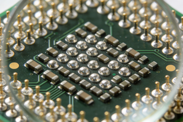
Escape Routing: From Traditional Dog-Bone to Advanced Via-in-Pad
4.1 Limits and Optimization of Dog-Bone Fanout
Traditional dog-bone layout is suitable for BGA pitches ≥0.8mm. Its core constraint is:
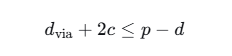
Where (c) is the minimum clearance (typically 0.1mm).
Optimization Techniques:
- Use oval pads to extend the connection neck.
- Control via diameter between 0.2-0.25mm.
- Use staggered routing on inner layers to improve channel utilization.
4.2 Via-in-Pad Technology
When pitch ≤0.65mm, via-in-pad becomes a necessary technology. TOPFAST offers two types of solutions:
Type VII Microvia (IPC-4761 Standard):
- Laser-drilled, diameter 0.1-0.15mm
- Resin-filled + copper cap planarization
- Supports the blind via structure, reducing inter-layer interference
Design Considerations:
- Pad Compensation: The area occupied by the via should be within 20% of the pad diameter.
- Solder Mask Treatment: Use solder mask plugging or fill planarization.
- Cost Trade-off: Microvias increase cost by 15-25% but improve routing density by 2-3 times.
Multi-Layer Stackup and Signal Integrity Co-Design
5.1 Stackup Architecture Planning
Empirical relationship between BGA pin count (Npins) and required layer count (Nlayers):
8-Layer Board Example Configuration:
| Layer | Function | Thickness | Notes |
|---|---|---|---|
| L1 | Signal + Pads | 0.1mm | Route the outermost 2 rows |
| L2 | Ground Plane | 0.2mm | Solid plane |
| L3/4 | Signal Layers | 0.15mm | Route rows 3-6 |
| L5/6 | Power Planes | 0.2mm | Split planes |
| L7 | Signal Layer | 0.15mm | Route remaining rows |
| L8 | Signal + Pads | 0.1mm | Bottom-side components |
5.2 Impedance Control and Crosstalk Suppression
Key Measures:
- Differential Pairs: Tightly coupled routing, length matching ≤5 mils.
- Reference Planes: Ensure signal layers are adjacent to solid planes.
- Via Back-Drilling: For signals >5GHz, eliminate stub effects.
- TOPFAST Special Process: Offers localized dielectric thickness adjustment to meet impedance accuracy of ±7%.
Manufacturing Processes and Reliability Validation
6.1 DFM Checklist
- Pad Size Tolerance: ±0.02mm (Laser Direct Imaging)
- Solder Mask Alignment: ±0.05mm (Confirm with manufacturer)
- Solder Paste Printing: Stencil aperture 0.05-0.1mm smaller than pad
- X-ray Inspection: Void rate <25% (IPC-A-610 Standard)
6.2 Reliability Test Items
TOPFAST recommended a three-stage verification process:
- Stage 1 Verification: Microsection analysis (via copper thickness, fill quality)
- Stage 2 Verification: Thermal cycling test (-55°C~125°C, 500 cycles)
- Stage 3 Verification: Interconnect resistance test (daisy chain monitoring)
Future Trends: Heterogeneous Integration and Advanced Packaging
With the development of Chiplet and 3D-IC technologies, BGA packaging is evolving towards:
- Silicon Interposer BGA: Supports multi-chip integration, improving interconnect density by 10x.
- Embedded Substrate BGA: Passives embedded, reducing area by 30-40%.
- Optoelectronic Integrated BGA: Supports optical channels, breaking electrical limits.
Conclusion
Successful BGA design requires traversing four dimensions:
- Electrical Dimension: Co-optimization of signal/power integrity.
- Thermal Dimension: Balance between thermal relief pads and overall heat dissipation.
- Mechanical Dimension: CTE matching and stress relief.
- Manufacturing Dimension: Optimal process capability and cost.
Based on experience from thousands of BGA projects, TOPFAST summarizes a four-step methodology: “Design – Simulation – Prototype – Mass Production,” which helps customers achieve yields of 90% or higher on their first design attempt. Remember: The finest-pitch BGA is not a technological showpiece, but the precise intersection of system requirements, design innovation, and manufacturing capability.
5 Common Q&As on BGA Package PCB Design
A: Core Principle:
Pad Size = Solder Ball Diameter × 0.85 ± Process Compensation
TOPFAST Recommended Values:
0.5mm pitch: Pad diameter 0.3-0.35mm
0.8mm pitch: Pad diameter 0.4-0.45mm
1.0mm pitch: Pad diameter 0.5-0.55mm
Key Considerations:
Use NSMD design (Solder mask opening 0.05mm larger than pad)
Must confirm process accuracy with the manufacturer
Clear marking for the A1 position is essential
A: Mandatory Usage:
Connection to large power/ground copper planes
High-current pins (>1A)
BGA corner positions
Optional Usage:
Signal pins typically use a direct connection
Low-current power pins
TOPFAST Recommended Parameters:
Number of spokes: 4
Spoke width: 0.15-0.25mm
Opening diameter: 0.3-0.5mm
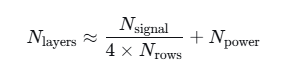
A: Layer Count Estimation Formula:
Layers ≈ (Number of pins requiring routing) ÷ (4 × Routable rows per layer) + 1 layer margin
TOPFAST Routing Strategy:
Outer layers: Route outermost 1-2 rows
Inner layers: Use dog-bone or via-in-pad
Key: Plan via locations early
Recommendations by Pitch:
≥0.8mm: Dog-bone fanout
0.65-0.8mm: Partial via-in-pad
≤0.5mm: Full via-in-pad
A: Four Key Points:
Impedance Control: Gradual taper from pad to trace
Crosstalk Suppression: High-speed signal spacing ≥ 3× trace width
Return Path: Provide ground via for each signal via
Power Integrity: Place decoupling capacitors within 50 mils of BGA
TOPFAST Checklist:
Differential pair length matching ≤ 5 mils
Impedance control within ±7%
Critical network crosstalk < -40dB
A: Design Stage:
Pad Surface Finish: ENIG (high-speed signals) or ImAg (cost-sensitive)
Stencil Design: Aperture size 85-90% of pad area
Spacing Check: Ensure minimum pad clearance requirements are met
Manufacturing Stage:
Solder paste printing inspection
X-ray inspection (void rate < 25%)
Reflow temperature profile verification
Electrical performance testing
TOPFAST Experience:
Involving the manufacturer in early DFM reviews can reduce mass production issues by over 70%. Providing BGA specifications to TOPFAST allows for customized process recommendations.