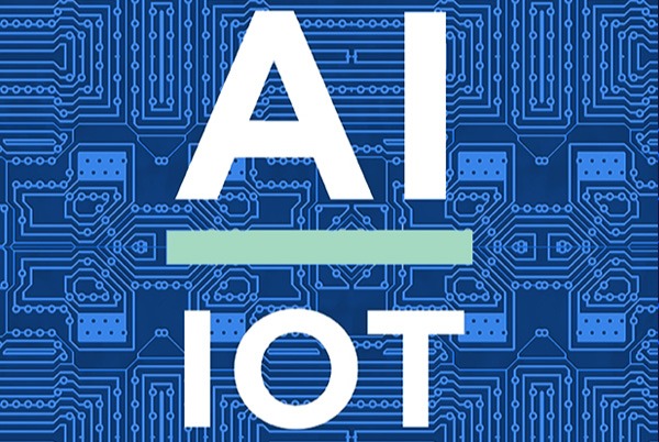
A silent revolution is taking place in the smart devices around us. When AI algorithms give machines the “ability to think,” and the Internet of Things (IoT) forms the “neural network,” the physical carrier for all this intelligence relies on that intricate Printed Circuit Board (PCB). The deep integration of these three elements is reshaping the face of every industry.
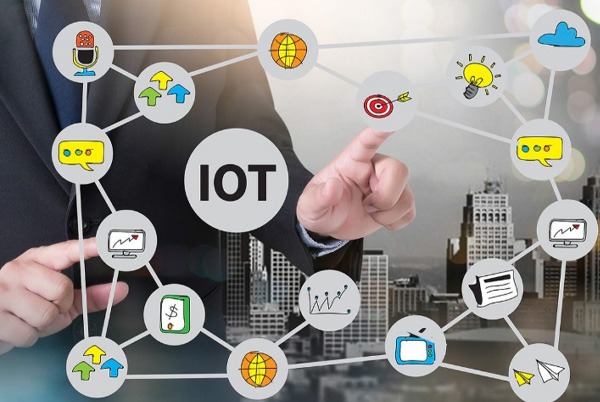
Table of Contents
The Intelligent Triad: AI is the Brain, IoT is the Nerves, PCB is the Skeleton
This triad constitutes the complete “life form” of modern intelligent devices:
| Role Division | Core Function | Implementation Carrier |
|---|---|---|
| AI (Brain) | Data Analysis, Intelligent Decision-Making, Pattern Recognition | AI Chips, Algorithm Models |
| IoT (Nerves) | Data Collection, Signal Transmission, Command Execution | Sensors, Communication Modules |
| PCB (Skeleton) | Function Integration, Signal Interconnection, Power Supply | Circuit Boards, Electronic Components |
Real-World Case:
- In smart factories, vibration sensors (IoT) collect data, edge AI chips analyze and predict equipment failures, and high-density PCBs ensure the stable operation of the entire system.
- Autonomous vehicles perceive the environment through LiDAR (IoT), the AI computing platform makes decisions within milliseconds, and specialized PCBs ensure system reliability in harsh environments.
How AI Empowers IoT Devices
1. The Leap from “Perception” to “Cognition”
Traditional IoT: Data Collection → Cloud Transmission → Simple Response
(e.g., Temperature sensor reports "Current temperature is 30°C")

AI-powered IoT: Data Collection → Local Analysis → Intelligent Decision-Making
(e.g., AI recognizes "Abrupt temperature spike," predicts equipment failure, and issues an early warning)
2. Edge Intelligence Becomes the New Trend
- Low Latency: Industrial robots require real-time response; edge AI ensures immediate command execution.
- Privacy Protection: Home security data is processed locally, avoiding privacy leaks.
- Bandwidth Optimization: Only key analysis results are uploaded, reducing network load.
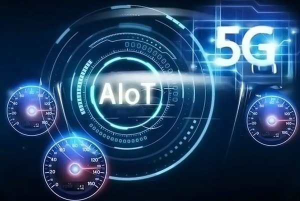
PCB Technology Innovation: Born for AIoT
Key Technological Breakthroughs:
▎ High-Density Interconnect (HDI) Technology
- Microvia Diameter: <0.1mm
- Line Width/Spacing: ≤0.075mm
- Outcome: Integration of a complete AI processing system into a space the size of a fingernail.
▎ Advanced Thermal Management Design
Problem: Significant increase in AI chip power density.
Solutions:
* Thermal Vias: Rapid heat conduction.
* Metal Core Substrates: Efficient heat dissipation.
* 3D Structures: Increased heat dissipation area.
▎ Mixed-Signal Integrity
- Digital Area: High-speed CPU/Memory Buses
- Analog Area: Precision Sensor Interfaces
- RF Area: 5G/Wi-Fi Communication Modules
- Innovative Solution: Zoning and Shielding Techniques to prevent mutual interference.
Challenges and Pathways to Breakthroughs
Challenge 1: The Ultimate Balance Between Computing Power and Power Consumption
Current Situation: High power consumption of AI inference vs. Need for long battery life in IoT devices.
Breakthrough Directions:
- Adoption of low-power AI chip architectures.
- Dynamic Voltage and Frequency Scaling (DVFS) technology.
- Intelligent power management algorithms.
Challenge 2: Reliability in Harsh Environments
Industrial Grade Standards Requirements:
- Operating Temperature: -40°C ~ 125°C
- Vibration Resistance: ≥5 Grms
- Service Life: ≥10 years
- Solutions: Specialized Materials, Enhanced Protection, Redundant Design.
Challenge 3: The Trade-off Between Cost and Performance
| Application Scenario | Cost Sensitivity | Performance Requirements | Technical Approach |
|---|---|---|---|
| Consumer Electronics | Very High | Medium | Optimized Design, Cost Reduction |
| Industrial Manufacturing | Medium | Very High | Ensure Reliability, Acceptable Cost |
| Medical Devices | Low | Very High | Optimal Performance, Cost is Secondary |
Future Outlook: A New Era of Intelligent Integration
Technology Convergence Trends:
- Heterogeneous Integration: Integrating chips from different manufacturing processes into a single package.
- Photoelectric Integration: Introducing optical interconnects to break through electrical performance bottlenecks.
- Self-Healing Systems: Devices automatically diagnose, predict, and repair potential faults.
Application Scenario Expansion:
- Smart Factories: AI Vision Inspection + IoT Monitoring + Industrial-grade PCB
- Smart Homes: Voice Interaction + Environmental Sensing + Consumer-grade PCB
- Intelligent Transportation: Autonomous Driving + V2X + Automotive-grade PCB
- Digital Healthcare: Health Monitoring + Remote Diagnosis + Medical-grade PCB
Conclusion: The deep integration of AI, IoT, and PCB is opening a new era for intelligent devices. This seemingly ordinary circuit board carries not just electronic components, but also the dreams and future of the intelligent age. As technology continues to break new ground, this “Intelligent Triad” will keep pushing the boundaries of innovation, making smart devices more understanding of our needs and better at serving our lives.