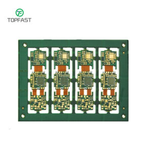
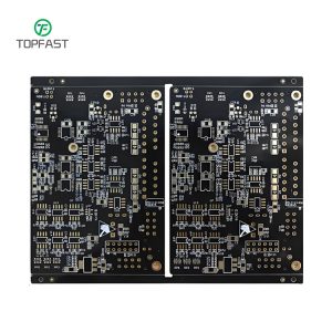
In today’s trend toward miniaturization and high performance in electronic products, high-density interconnect (HDI) circuit boards have become the core carrier for high-end electronic devices. Their exceptional performance relies on extremely precise manufacturing processes and rigorous inspection standards to ensure the quality and reliability of HDI boards.
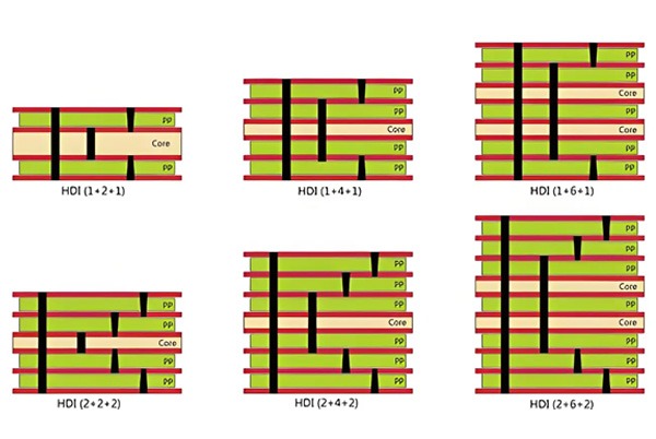
Table of Contents
Understanding HDI
Before delving into the inspection standards, it is essential to understand what makes HDI boards unique. The core of HDI technology lies in the use of Build-up Manufacturing, extensively employing microvias, fine lines, and thin dielectric layers.
- Core Structure: Typically uses a conventional core as support, alternately laminating build-up layers and copper foils on it, with interlayer connections achieved through microvias.
- Key Terminology:
- Microvia: A blind or buried via with a diameter ≤ 0.15mm, key to achieving high-density interconnect.
- Target Pad & Capture Pad: The connection pads at the bottom and top of a microvia, respectively.
- Buried Via: A conductive via completely hidden within the board, not extending to the outer surfaces.
To better understand, the following diagram illustrates a typical HDI board stack-up:
+-----------------------------------------------------------------+
| << Outer Solder Mask >> | << Surface Copper >> | << Top Build-up >> |
|-------------------------|----------------------|-------------------|
| << Microvia >> -------> | Connects to | << Capture Pad >>   |
|-------------------------|----------------------|-------------------|
| << Laser Drillable Prepreg >> or << Resin Coated Copper >>       |
|-------------------------|----------------------|-------------------|
| << Target Pad >> | <--- Connects to | << Buried Via >>     |
|-------------------------|----------------------|-------------------|
| << Core >> (Potentially multi-layered, containing buried vias)   |
|-------------------------|----------------------|-------------------|
| << Bottom Build-up >> | << Bottom Copper >> | << Outer Solder Mask >> |
+-----------------------------------------------------------------+
(Schematic: Shows the relationship between core, build-up layers, microvias, buried vias, and target/capture pads in an HDI board.)
The Hierarchy of HDI Inspection Standards
When technical requirement conflicts arise, the following hierarchy (from highest to lowest priority) should be followed to ensure the final product meets design intent:
- Highest Priority: Customer-provided Design Files and Approved Technical Agreements.
- Second Priority: Specific HDI Inspection Standards (as described in this document).
- Foundation Priority: General Rigid PCB Inspection Standards and IPC International Standards.
Key Inspection Points Throughout the HDI Manufacturing Process
1. Material Inspection:
HDI boards have extremely stringent material requirements, forming the basis for all subsequent processes.
| Material Type | Key Inspection Items | Standard Requirements |
|---|---|---|
| Core & Build-up Dielectric | Material Type, Tg, Dk, Df | The default core is FR-4. Build-up dielectric is recommended to be RCC or LDP. All materials must meet relevant performance standards. |
| Copper Foil | Thickness, Tensile Strength, Elongation, Surface Roughness | RCC foil is commonly 1/2 oz or 1/3 oz, requiring excellent mechanical and electrical properties. |
| Metallic Plating | Microvia Copper Thickness | This is critical for HDI reliability! Grade A requires ≥10μm, Grade B requires ≥5μm, ensuring microvias do not crack under thermal stress. |
2. Structural & Visual Inspection
This phase of inspection focuses on the physical results of manufacturing, typically performed using microscopes, AOI, etc.
- Microvia Quality:
- Shape: Check for an ideal conical shape, avoiding defects like “nail heading”.
- Filling: For filled microvias, require sufficient fill with surface depression depth conforming to standards.
- Registration: Microvias must land completely on the Target Pad below, without pad violation.
- Circuitry & Surface:
- Line Width/Space: Measure deviation from design values to ensure fine line integrity.
- Surface Finish: Whether ENIG, Immersion Tin, or OSP, inspect for thickness, uniformity, and solderability.
- Solder Mask: Check for coating uniformity, registration accuracy, ensuring no seepage, poor exposure, etc.
3. Electrical & Reliability Testing
This is the core stage for verifying HDI board functionality and durability.
- Electrical Performance Testing:
- Continuity/Insulation Test: Use a flying probe or dedicated fixtures for 100% open/short circuit verification.
- Impedance Control: For high-speed lines, perform sample testing of characteristic impedance to ensure it falls within design tolerance.
- Reliability Testing (Environmental Stress Screening):
- Thermal Stress Test: Refer to IPC-TM-650 methods for multiple thermal cycles or thermal shock, followed by microsectioning analysis to check for plating cracks, delamination.
- Interconnect Stress Test: Specifically designed to evaluate the long-term reliability of microvias under current load.
- Solderability Test: Evaluate the solder wetting ability of pads to prevent cold solder joints, poor wetting.

Overview of Professional Inspection Methods & Tools
| Inspection Category | Common Methods & Tools | Inspection Purpose |
|---|---|---|
| Visual & Structural | Automated Optical Inspection, CMM, Metallurgical Microscope | Detect microvia/line defects, measure dimensions |
| Internal Structure | Microsectioning Analysis, X-Ray Inspection | Observe copper thickness, lamination integrity, and check internal layer registration |
| Electrical Performance | Flying Probe Tester, Impedance Tester, Network Analyzer | Test continuity, insulation, impedance, and high-frequency performance |
| Reliability | Thermal Cycle Chamber, THB Chamber, Peel Strength Tester | Assess product lifespan and stability under harsh environments |
Conclusion
The inspection of HDI circuit boards is far from a simple pass/fail determination; it is a systematic process that spans the entire lifecycle from design and material selection to manufacturing. Only through the rigorous implementation of a multi-level, multi-dimensional inspection system—covering everything from materials to reliability—can we truly ensure that every HDI circuit board delivers stable, enduring, and exceptional performance within the final product.