Copper plating is a critical step that turns drilled holes into reliable electrical connections.
No matter how well a PCB is designed, poor copper plating can lead to:
- Intermittent connections
- Via cracking
- Premature product failure
From a manufacturer’s perspective, copper plating is not just a chemical process—it is a reliability gate.
This article explains how copper plating works in PCB manufacturing, the different plating stages, and how manufacturers like TOPFAST control plating quality to ensure long-term performance.
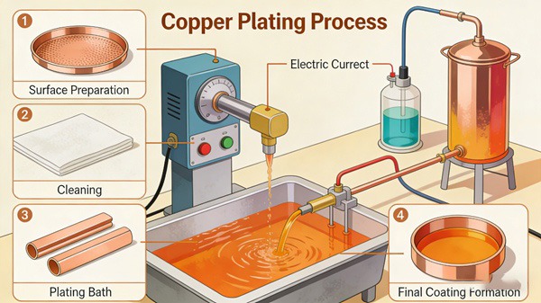
Table of Contents
What Is Copper Plating in PCB Manufacturing?
Copper plating is the process of depositing copper onto PCB surfaces and inside drilled holes to create electrical connections between layers.
Plating serves two main purposes:
- Enable electrical continuity through vias
- Achieve the required copper thickness for current and reliability
Types of Copper Plating in PCB Manufacturing
Electroless Copper Plating
Electroless copper plating deposits a thin, uniform copper layer without using electrical current.
Purpose
- Create an initial conductive layer inside drilled holes
- Prepare the PCB for electroplating
Typical thickness:
- ~1–3 microns
This step is essential for making vias electrically functional.
Electrolytic Copper Plating
Electroplating uses electrical current to build up copper thickness.
Purpose
- Strengthen via walls
- Increase surface copper thickness
- Meet design copper specifications
Electroplating determines:
- Via reliability
- Current-carrying capacity
- Mechanical strength
Step-by-Step Copper Plating Process
Step 1 – Hole Wall Preparation
After drilling, the hole walls must be:
- Cleaned
- Desmeared
- Activated for copper deposition
Poor preparation leads to weak copper adhesion.
Step 2 – Electroless Copper Deposition
A thin copper layer is deposited chemically, ensuring:
- Uniform coverage
- Electrical continuity
This layer is the foundation for all subsequent plating.
Step 3 – Electroplating Thickness Build-Up
Copper thickness is increased through controlled electroplating.
Key parameters include:
- Current density
- Bath chemistry
- Temperature
- Plating time
Consistency here is crucial for reliability.
Plating Thickness and Why It Matters
Via Wall Thickness
Via reliability depends heavily on:
- Minimum copper thickness
- Uniform distribution
Insufficient copper can cause:
- Cracks during thermal cycling
- Open circuits
Surface Copper Thickness
Surface copper affects:
- Trace current capacity
- Etching performance
- Impedance control
At TOPFAST, plating thickness is carefully matched to design requirements to avoid over- or under-plating.
Common Copper Plating Defects
H3: Thin Plating
Caused by:
- Insufficient plating time
- Poor current distribution
Results in reduced reliability.
Void Formation
Voids inside vias can occur due to:
- Poor hole cleaning
- Incomplete electroless coverage
Voids are a major reliability risk.
Uneven Plating
Uneven copper distribution leads to:
- Weak via walls
- Impedance variation
- Yield loss
How Copper Plating Affects PCB Reliability
Copper plating quality directly impacts:
- Thermal cycling performance
- Mechanical stress resistance
- Long-term electrical stability
In high-reliability applications, plating quality often matters more than board appearance.
Design Factors That Influence Plating Quality
From a manufacturing perspective, plating becomes more challenging when:
- The aspect ratio is too high
- The hole size is too small
- Copper distribution is uneven
- Heavy copper designs are used
Early DFM review helps identify plating risks before production.
Manufacturer’s Perspective: How TOPFAST Controls Plating Quality
At TOPFAST, copper plating quality is ensured through:
- Controlled chemical bath management
- Real-time thickness monitoring
- Regular cross-section analysis
- IPC-aligned acceptance standards
- DFM-driven design feedback
The focus is on stable yield and long-term reliability, not just meeting minimum specifications.
Cost Considerations of Copper Plating
Copper plating cost increases with:
- Heavy copper requirements
- High aspect ratio vias
- Tight thickness tolerances
- Advanced reliability specifications
Optimising plating requirements can significantly reduce PCB cost without compromising performance.
Conclusion
Copper plating is one of the most critical processes in PCB manufacturing.
It transforms drilled holes into durable electrical connections and defines PCB reliability.
By understanding how copper plating works and what affects its quality, designers and buyers can make smarter decisions that balance cost, performance, and reliability.
With controlled processes and manufacturing expertise, TOPFAST ensures copper plating quality that supports reliable PCB performance throughout the product lifecycle.
Related Reading
PCB Manufacturing Process Explained Step by Step
Inner Layer Fabrication Explained
PCB Drilling vs Laser Drilling
Copper Plating FAQ
A: Copper plating creates electrical connections between PCB layers and ensures sufficient copper thickness for reliability.
A: Electroless plating creates an initial conductive layer, while electrolytic plating builds copper thickness using electrical current.
A: Via copper thickness depends on design and reliability requirements, but must meet IPC standards for long-term performance.
A: Voids are typically caused by poor hole cleaning or incomplete electroless copper coverage.
A: Proper copper plating improves resistance to thermal stress, mechanical fatigue, and electrical failure.