High Frequency PCB Design and Layout Guide
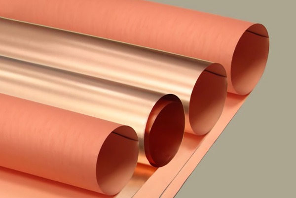
High-frequency PCB board refers to the electromagnetic frequency of the higher special circuit boards for high-frequency (frequency greater than 300MHZ or wavelength of less than 1 meter) and microwave (frequency greater than 3GHZ or wavelength of less than 0.1 meters) in the field of PCB, is in the microwave substrate copper-clad laminate boards on the use of ordinary rigid circuit boards manufactured using some of the processes or the use of special treatment methods and the production of circuit boards.
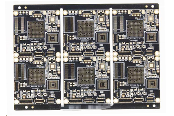
Table of Contents
High-frequency PCB layout and wiring design specifications
1.Isolation and grounding principles
- Strictly separate digital and analog circuit areas
- Ensure that all RF alignments have a complete ground plane reference.
- Prioritize the surface layer alignment for RF signal transmission
2.Wiring Priority Order
RF lines → baseband RF interface lines (IQ lines) → clock signal lines → power lines → digital baseband circuits → ground network
3.Surface treatment specification
- High-frequency single-board (>1GHz) is recommended to eliminate the green oil cover in the microstrip line area.
- Low and medium frequency single board microstrip line is recommended to retain the green oil protective layer
4.Cross wiring specification
- Strictly prohibit digital/analog signal cross-wiring.
- RF lines and signal lines need to be met when crossing:
a) Preferred option: add an isolated ground plane layer
b) Second choice: Maintain 90° orthogonal crossings. - Parallel RF line spacing requirements:
a) Normal wiring: Maintain 3W spacing.
b) When parallelism is necessary, insert a well-grounded isolated ground plane in the center.
5.Mixed Signal Processing
- Duplexers/mixers and other multi-signal devices are required:
a) RF/IF signals are routed orthogonally.
b) Isolated ground barrier between signals
6.Alignment Integrity Requirements
- Overhanging ends of RF alignment are strictly prohibited.
- Maintain transmission line characteristic impedance consistency
7.Vias Handling Specifications
- Avoid changing layers of RF alignment as much as possible.
- When a layer change is necessary:
a) Use the smallest hole size (recommended 0.2mm)
b) Limit the number of vias (≤ 2 per line)
8.Baseband interface wiring
- IQ line width ≥ 10 mil
- Strict equal length matching (ΔL ≤ 5 mil)
- Maintain uniform spacing (±10% tolerance)
9.Control line wiring
- Route length optimized for termination impedance
- Minimize proximity to the RF path
- Prohibit the placement of ground vias next to control wires
10.Interference protection
- 3H spacing between digital/power supply alignments and RF circuits (H is the thickness of the dielectric)
- Separate shielding area for clock circuits
11.Clock wiring
- Clock wiring ≥ 10 mils
- Double-sided grounded shielding
- Ribbon wire structure is preferred
12.VCO wiring
- Control lines ≥2mm from RF lines
- If necessary, implement full ground wrap treatment
13.Multilayer design
- Prefer a cross-layer isolation scheme
- The second choice of the orthogonal crossover solution
- Limit parallel length (≤λ/10)
14.Grounding System
- Ground plane completeness of each layer >80
- Grounding hole spacing <λ/20
- Multi-point grounding in critical areas
Note: All dimensional specifications should be adjusted according to the wavelength (λ) of the actual operating frequency, and it is recommended that three-dimensional electromagnetic field simulation be carried out to verify the final design.

High-speed high-frequency PCB key performance parameters technical specifications
1.Dielectric Characteristic Parameters
1.1 Dielectric constant (Dk)
- Typical requirement: 2.2-3.8 (@1GHz)
- Key Indicator:
- Numerical stability (±0.05 tolerance)
- Frequency dependence (<5% variation from 1-40 GHz)
- Isotropy (X/Y/Z axis variation <2%)
1.2Dielectric loss (Df)
- Standard range: 0.001-0.005 (@10GHz)
- Core Requirements:
- Low loss characteristics (Df <0.003 preferred)
- Temperature stability (-55℃~125℃ variation <15%)
- Surface roughness impact (Ra <1μm)
2.Thermo-mechanical properties
2.1 Coefficient of thermal expansion (CTE)
- Copper foil matching requirements:
- X/Y axis CTE: 12-16ppm/°C
- Z-axis CTE: 25- 50 ppm/°C
- Reliability standard:
- 300 thermal cycles (-55℃~125℃) without delamination
2.2 Heat resistance index
- Tg point: ≥170℃ (preferably 180-220℃)
- Td point: ≥300℃ (5% weight loss temperature)
- Delamination time: >60min (288℃ solder test)
3.Environmental stability
3.1 Moisture absorption characteristics
- Saturated water absorption: <0.2% (24h immersion)
- Dielectric parameter drift:
- Dk change <2%
- Df change <10%
3.2 Chemical resistance
- Acid and alkali resistance: 5% concentration solution immersion 24h without corrosion
- Solvent resistance: Passed IPC-TM-650 2.3.30 test.
4.Electrical Performance
4.1 Impedance control
- Single-ended line: 50Ω±10%.
- Differential pairs: 100Ω±7%
- Key control points:
- Tolerance of line width ±5%
- Tolerance of dielectric thickness ±8%
- Copper Thickness Tolerance ±10
4.2 Signal Integrity
- Insertion loss: <0.5dB/inch@10GHz
- Return Loss: >20dB@Operating Band
- Crosstalk rejection: <-50dB@1mm spacing
5.Mechanical Reliability
5.1 Peel Strength
- Initial value: >1.0N/mm
- After thermal aging: >0.8N/mm (125℃/1000h)
5.2 Impact strength
- CAF resistance: >1000h (85℃/85%RH/50V)
- Mechanical shock: Pass 30G/0.5ms test
6.Special Performance Requirements
6.1 High Frequency Stability
- Phase consistency: ±1°@10GHz/100mm
- Group delay: <5ps/cm@40GHz
6.2 Surface Finish
- Copper foil roughness: Rz<3μm
- Soldermask effect: Dk variation <1%
Notes:
- All parameters should be tested according to IPC-TM-650 standard methods.
- Batch sampling is recommended for key parameters.
- High frequency application should provide Dk/Df with a frequency variation curve.
- Multilayer boards should be evaluated for Z-axis parameter consistency.
High-Frequency PCB Material Dk/Df Testing Technical White Paper
1. Classification and Selection Principles of Testing Methods
1.1 Testing Method System
- IPC Standard Methods: 12 standardized testing protocols
- Industry Custom Methods: Proprietary solutions from research institutions and manufacturers
- Practical Selection Criteria:
• Frequency matching (±20% of operating band)
• Electric field direction consistency (Z-axis/XY plane)
• Correlation with manufacturing processes (raw material/finished board)
1.2 Method Selection Matrix
| Testing Requirement | Recommended Method | Application Scenario |
|---|---|---|
| Raw material evaluation | Fixture-based method | Incoming inspection |
| Finished board validation | Circuit testing method | Design verification |
| Anisotropy analysis | Combined testing approach | High-frequency material research |
2. Detailed Explanation of Core Testing Techniques
2.1 X-Band Clamped Stripline Resonator Method (IPC-TM-650 2.5.5.50)
- Test Structure:
┌─────────────────┐
│ Ground Plane │
├─────────────────┤
│ DUT (Z-axis) │
├─────────────────┤
│ Resonator Circuit│
├─────────────────┤
│ DUT (Z-axis) │
├─────────────────┤
│ Ground Plane │
└─────────────────┘ - Technical Characteristics:
• Frequency range: 2.5–12.5 GHz (increments of 2.5 GHz)
• Accuracy: ±0.02 (Dk), ±0.0005 (Df)
• Error sources: Fixture air gaps (~1–3% deviation)
2.2 Split Cylinder Resonator Method (IPC-TM-650 2.5.5.13)
- Key Parameters:
• Testing direction: XY-plane properties
• Resonance peaks: 3–5 characteristic frequency points
• Anisotropy analysis: Can compare with Z-axis data
2.3 Microstrip Ring Resonator Method
- Circuit Requirements:
• Feedline impedance: 50Ω ±1%
• Ring gap: 0.1–0.15 mm (requires lithography control)
• Copper thickness tolerance: ±5 μm compensation needed
3. Test Error Analysis and Compensation
3.1 Major Error Sources
- Material Dispersion: Frequency-dependent Dk (typical: -0.5%/GHz)
- Copper Roughness Impact: Roughness Level Dk Deviation Rz < 1 μm <1% Rz = 3 μm 3–5% Rz > 5 μm >8%
- Process Variations:
• Plated copper thickness (0.3% error per 10 μm deviation)
• Solder mask influence (0.5–1.2% variation due to green oil coverage)
3.2 Data Correction Methods
- Frequency Compensation Algorithm:
Dk(f)=Dko⋅(1−α⋅log(f/fo)) - Surface Roughness Correction: Hammerstad-Jensen model
- Anisotropic Material Handling: Tensor analysis method
4. Engineering Application Guidelines
4.1 Testing Plan Development Process
- Determine operating frequency band (center frequency ±30%)
- Analyze primary electric field direction (microstrip/stripline)
- Evaluate manufacturing process window (copper thickness/line width tolerance)
- Select a testing method with >80% matching accuracy
4.2 Data Comparison Standards
- Valid Comparison Conditions:
• Same testing direction (Z-axis or XY plane)
• Frequency deviation < ±5%
• Consistent temperature conditions (23±2°C) - Typical Material Parameter Variations: Testing Method Dk Variation Df Variation Fixture vs. Circuit 2–8% 15–30% Z-axis vs. XY Plane 1–15% 5–20%
5. Evolution of Testing Standards
5.1 Emerging Testing Technologies
- Terahertz time-domain spectroscopy (0.1–4 THz)
- Near-field scanning microwave microscopy (10–100 GHz)
- AI-assisted parameter extraction systems
5.2 Standardization Trends
- Multilayer board testing methods (IPC-2023 draft)
- 5G mmWave-specific testing protocols (28/39 GHz)
- Dynamic thermal cycling test standards
Note: All tests should be conducted in a controlled environment (23±1°C, 50±5% RH). Automated test systems integrating vector network analyzers (VNA) and probe stations are recommended. Test data must include 3σ statistical analysis.





Related Posts