How to determine if a PCB is soldered correctly?
Table of Contents
Why is PCB Soldering Quality So Important?
In electronics manufacturing, PCB soldering quality directly determines the performance and product life of circuit boards. A tiny cold solder joint or short circuit can cause the entire device to fail. So, how can we ensure that PCB soldering is done correctly?
7 Professional PCB Soldering Inspection Methods
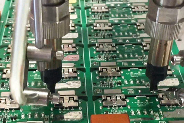
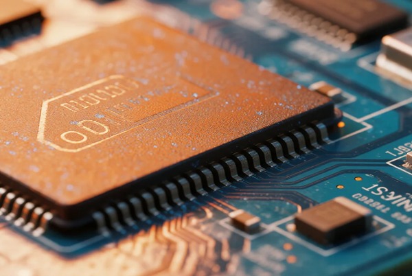
1. Visual Inspection (Manual/AOI)
Applicable Scenario: Quick screening for obvious soldering defects
- Manual Inspection: Check if solder joints are smooth, rounded, and free of cold solder joints, cracks, or solder bridges.
- AOI (Automated Optical Inspection): Uses high-precision cameras to compare solder joints with standard images, identifying size, shape, or color anomalies. Ideal for batch inspection.
AOI can detect over 80% of surface defects but cannot identify hidden solder joints like those in BGA components.
2. X-Ray Inspection (Detecting Hidden Defects)
Applicable Scenario: BGA, QFN, and other hidden solder joints
- Uses X-rays to examine internal solder joint structures, detecting voids, cold solder joints, or ball misalignment.
- Particularly suitable for high-density PCBs and micro-component soldering quality assessment.
If you need high-precision PCB soldering inspection services, TopFast PCB offers professional X-ray inspection to ensure zero defects in your circuit boards.
3. Flying Probe Testing (Electrical Performance Verification)
Applicable Scenario: Small-batch or prototype board testing
- Uses movable probes to measure solder joint resistance—cold solder joints result in abnormally high resistance.
- No custom fixtures needed; flexible and efficient, but slower.
4. In-Circuit Testing (ICT) (Comprehensive Circuit Verification)
Applicable Scenario: Mass production
- Uses test fixtures to check the connectivity and functionality of all components.
- Quickly locates shorts, opens, or component value deviations.
5. Functional Testing (FCT)
Applicable Scenario: Final product acceptance
- Simulates real-world operating conditions to validate overall PCB performance.
- Ensures soldering defects do not affect actual functionality.
6. Thermal Imaging Inspection (Identifying Overheated Solder Joints)
Applicable Scenario: High-power circuit boards
- Uses infrared cameras to detect localized overheating, indicating cold solder joints or poor contact.
7. Environmental Stress Testing (Reliability Verification)
Applicable Scenario: High-standard products (e.g., military, automotive electronics)
- Includes temperature cycling, vibration testing, etc., to ensure solder joint reliability under extreme conditions.
TopFast PCB provides end-to-end quality control services from design to production, helping your products pass rigorous environmental tests.
Common Soldering Defects and Solutions
| Defect Type | Symptoms | Solution |
|---|---|---|
| Cold Solder Joint | Dull, loose solder joint | Re-solder with proper temperature and time control |
| Solder Bridge | Short circuit between adjacent joints | Remove excess solder with desoldering braid |
| Pad Lifting | Copper foil separates from the substrate | Replace the pad or repair the trace |
| Voiding | Internal bubbles in the solder joint | Optimize the reflow soldering temperature profile |
How to Choose Inspection Methods?
Small-Batch Production: Flying probe testing + functional testing
Mass Production: AOI + ICT + X-ray sampling
High-Reliability Requirements: Full-process inspection (AOI + X-ray + environmental testing)
PCB soldering quality is the lifeline of electronic products. By combining multiple inspection methods, you can comprehensively control soldering defects and ensure the high reliability of circuit boards. If you are looking for professional PCB manufacturing and inspection services, contact the TopFast PCB team, and we will provide you with a one-stop solution!


Related Posts