Japan’s contribution to the electronics world is defined by Monozukuri (the art of making things). The Japanese PCB industry is not just about production; it is about the relentless pursuit of miniaturization and reliability. From the robotics clusters in Nagoya to the semiconductor giants in Kyushu, Japanese engineers set the global gold standard for High-Density Interconnect (HDI) and Flexible PCB technology.
For international firms sourcing from Japan, or Japanese firms looking to scale, the focus is always on one thing: Quality without compromise.
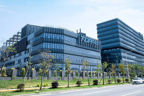
Table of Contents
The Japanese PCB Landscape: Micro-Precision & Advanced Materials
Japan is home to the world’s most advanced material science companies (like Panasonic, Mitsubishi, and Taiyo), which gives local fabricators a unique edge. Key strengths of the Japanese market include:
Zero-Defect Culture: A rigorous inspection culture that often goes far beyond standard IPC Class 2 or 3 requirements.
Extreme Miniaturization: Expertise in Any-layer HDI and 25μm trace/space technology for next-gen smartphones and wearable medical devices.
High-Performance Substrates: Direct access to specialized low-loss materials (like Panasonic Megtron series) is essential for 6G and AI computing.
Top PCB Manufacturers in Japan
| Manufacturer | Core Strength | Strategic Value |
| Meiko Electronics | Automotive & High-Volume | A leader in MSAP (Modified Semi-Additive Process) for fine-line designs. |
| CMK Corporation | Automotive PCB | Deep integration with Japanese Tier 1 automotive supply chains. |
| Nippon Mektron | Flexible PCBs (FPC) | The global leader in high-end Flexible PCB manufacturing. |
| Kyoden | Quick-turn R&D | Specialized in ultra-fast prototyping for Japanese robotics startups. |
Technical Expectations for the Japanese Market
If you are designing for a Japanese client or using Japanese components, your PCBs must meet these specific aesthetic and functional benchmarks:
Gold Plating Quality: For high-reliability sensors, ENIG or ENEPIG finishes must be flawless to ensure long-term wire bonding stability.
Solder Mask Perfection: Japanese QC typically rejects boards with uneven solder mask thickness or slight misalignments that Western standards might accept.
Material Traceability: Preference is often given to domestic Japanese laminates. Ensuring your supplier can source authentic Panasonic Megtron 6/7 or Hitachi materials is crucial for High-Speed PCB projects.
Why TopFast is the Trusted Partner for Japanese Engineering
We understand that for our Japanese clients, a “good” board is not enough—it must be perfect. TopFast provides a bridge between Japanese quality expectations and global manufacturing efficiency:
Cross-Border Logistics: We handle all specialized documentation for smooth entry into Japanese ports (Narita/Kansai), ensuring your “Just-in-Time” (JIT) production schedules are never compromised.
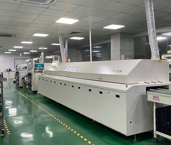
Adoption of Japanese Standards: Our production lines are optimized to meet the strict cosmetic and functional criteria expected by Japanese “Sensei” engineers. Our Quality Control includes 100% AOI and optional four-terminal sensing for low-resistance testing.
Specialized Material Inventory: We maintain direct supply chains for Japanese-origin laminates, ensuring that your HDI PCB designs perform exactly as simulated.
PCB Manufacturing by Region
TOPFAST PCB also provides tailored PCB manufacturing services for other regions:
Japan PCB Manufacturer FAQ
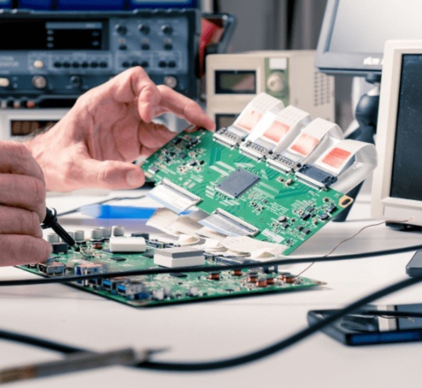
A: Yes. We provide comprehensive outgoing inspection reports, including micro-sectioning analysis, copper thickness measurements, and ionic contamination results tailored to Japanese documentation standards.
A: Absolutely. We specialize in High-Mix Low-Volume (HMLV) orders, allowing Japanese startups to access Advanced PCB Assembly without the prohibitive costs of local domestic mass-production.
A: We provide full Material Certifications (CoC) from the original manufacturers like Panasonic or Taiyo, ensuring that every layer of your board meets the specified dielectric constant (Dk) and dissipation factor (Df).