PCB Materials and Panelization Basics
Table of Contents
1. PCB Material Fundamentals
1.1 Core Components of PCB Materials
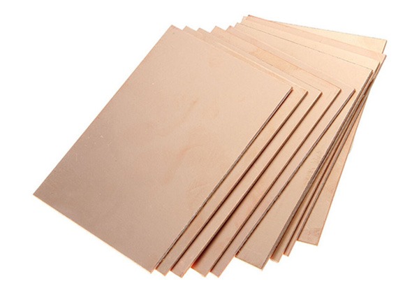
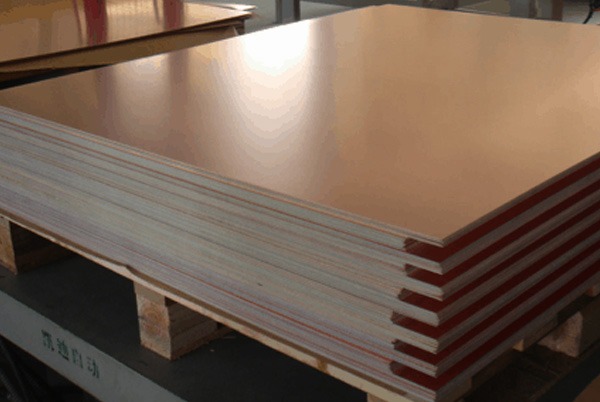
PCB materials, known as Copper-Clad Laminates (CCL), form the substrate for manufacturing printed circuit boards, directly determining the board’s electrical performance, mechanical properties, thermal characteristics, and manufacturability.
| Component | Function & Characteristics | Material Composition |
|---|---|---|
| Insulating Layer | Provides electrical insulation and mechanical support | Epoxy resin, fiberglass cloth, PTFE, etc. |
| Conductive Layer | Forms circuit connection paths | Electrolytic copper foil, rolled copper foil (typically 35-50μm thick) |
1.2 Common PCB Material Types and Applications
FR-4 Material
- Composition: Fiberglass cloth + Epoxy resin
- Characteristics: Cost-effective, balanced mechanical and electrical properties, flame-retardant
- Applications: Consumer electronics, computer motherboards, industrial control boards, and most common electronic products
High-Frequency/High-Speed Materials
- Composition: PTFE, hydrocarbons, ceramic fillers
- Characteristics: Extremely low dielectric constant (Dk) and dissipation factor (Df), minimal signal transmission loss, excellent stability
- Applications: 5G base station antennas, satellite communications, high-speed network equipment, automotive radar
Metal Core Substrates
- Composition: Thermally conductive insulating layer + aluminum/copper substrate
- Characteristics: Excellent heat dissipation performance, high thermal conductivity
- Applications: LED lighting, power modules, power amplifiers, automotive headlights
1.3 Key Performance Parameters of PCB Materials
Thermal Performance Indicators
- Tg (Glass Transition Temperature)
- Standard FR-4 Tg: 130°C – 140°C
- Mid-Tg FR-4: 150°C – 160°C
- High-Tg FR-4: ≥ 170°C (suitable for lead-free soldering processes)
- Td (Decomposition Temperature)
- The temperature at which the substrate begins chemical decomposition
- Higher Td indicates better high-temperature stability
Electrical Performance Indicators
- Dk (Dielectric Constant)
- Affects signal propagation speed and impedance in the dielectric medium
- Lower Dk values enable faster signal propagation
- Df (Dissipation Factor)
- Energy loss when signals propagate through the dielectric medium
- Lower Df values indicate reduced signal loss
Mechanical Reliability Indicators
- CTE (Coefficient of Thermal Expansion)
- Z-axis (thickness direction) CTE should be minimized to prevent barrel cracking after multiple reflow cycles
- CAF Resistance
- Prevents conductive anodic filament formation under high temperature and humidity conditions
2. Detailed PCB Panelization Process
2.1 Standard Panel Sizes
Standard original sizes from PCB material suppliers serve as basic procurement and inventory units for PCB manufacturers:
| Size Type | Common Specifications | Applicable Materials |
|---|---|---|
| Mainstream Sizes | 36″ × 48″, 40″ × 48″, 42″ × 48″ | FR-4 and other rigid materials |
| Custom Sizes | Tailored to customer requirements | High-frequency boards, metal core boards |
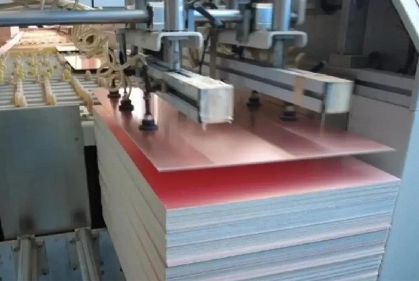
2.2 Production Panel Size Optimization
PCB manufacturers cut standard panels into smaller production panels suitable for production line processing through panelization, with the core objective of maximizing material utilization.
Panelization Optimization Strategies:
- Use specialized layout software for optimal panel utilization
- Consider equipment processing capability limitations
- Balance production efficiency with material utilization
2.3 Key Factors Influencing Production Panel Sizes
- Equipment Processing Capabilities: Size limitations of exposure machines, etching lines, presses, etc.
- Production Efficiency Considerations: Moderate sizes improve production rhythm and yield rates
- Material Utilization: Core consideration directly impacting cost control
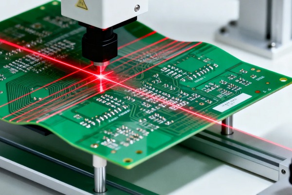
3. Detailed PCB Layer Structure and Functions
3.1 Comprehensive PCB Layer Structure Overview
| Layer Type | Function Description | Visual Characteristics |
|---|---|---|
| Silkscreen Layer | Marks component designators and outlines | White characters (when the solder mask is green) |
| Solder Mask Layer | Insulation protection prevents short circuits | Green or other colored ink (negative image) |
| Solder Paste Layer | Assists with soldering, improves solderability | Tin or gold plating on pads (positive image) |
| Electrical Layer | Signal routing, electrical connections | Copper traces, internal planes in multilayer boards |
| Mechanical Layer | Physical structure definition | Board outline, slots, and dimension markings |
| Drill Layer | Drill data definition | Through holes, blind vias, and buried vias locations |
3.2 In-depth Analysis of Key Layers
Solder Mask and Solder Paste Layer Relationship
- Mutual Exclusion Principle: Areas with solder mask have no solder paste, and vice versa
- Design Essentials: Solder mask uses negative image design, solder paste uses positive image design
Electrical Layer Design Strategy
- Single-layer Boards: Only one conductive layer
- Double-layer Boards: Top and bottom conductive layers
- Multilayer Boards: 4 layers or more, inner layers can be set as power and ground planes using a negative image
Mechanical Layer vs. Silkscreen Layer Differences
- Different Purposes: Silkscreen aids component identification; mechanical layer guides PCB manufacturing and physical assembly
- Content Differences: Silkscreen primarily contains text and symbols; the mechanical layer includes physical dimensions, drill locations, etc.
4. Practical PCB Design Guide
4.1 Component Package Basics
Essential Package Considerations:
- Accurately match physical component dimensions
- Distinguish between through-hole (DIP) and surface-mount (SMD) packages
- Numbers like 0402, 0603 represent component dimensions (unit: inches)
4.2 Power Supply Design Selection
Switching vs. Linear Power Supplies
| Power Type | Advantages | Disadvantages | Application Scenarios |
|---|---|---|---|
| Switching Power Supply | High efficiency (80%-95%) | Large ripple, complex design | High-power applications, battery-powered devices |
| Linear Power Supply | Low ripple, simple design | Low efficiency, significant heat generation | Low-power, noise-sensitive circuits |
| LDO | Low dropout, low noise | Still relatively low efficiency | Low dropout applications, RF circuits |
4.3 Standardized PCB Design Process
Phase 1: Schematic Design
- Component Library Preparation
- Create packages based on actual component dimensions
- Recommended to use established libraries like JLCPCB
- Add 3D models for visual verification
- Circuit Schematic Drawing
- Reference application circuits provided by chip manufacturers
- Learn from proven module designs
- Utilize online resources (CSDN, technical forums) for reference designs
Phase 2: PCB Layout and Routing
- Component Placement Guidelines
- Compact placement of functional modules
- Keep heat-generating components away from sensitive devices
- Follow layout recommendations in chip datasheets
- Signal Routing Specifications
- Trace width: 10-15mil (regular signals)
- Avoid acute and right-angle traces
- Place crystals close to ICs with no traces underneath
- Power and Ground Plane Management
- Power trace width: 30-50mil (adjusted based on current)
- Ground connections can be achieved through copper pouring
- Use vias appropriately to connect different layers
5. Professional Design Techniques and Considerations
5.1 High-Speed Circuit Design Essentials
- Impedance Matching: 50Ω single-ended, 90/100Ω differential
- Signal Integrity: Consider transmission line effects, control reflections, and crosstalk
- Power Integrity: Adequate decoupling capacitor placement
5.2 Thermal Management Strategies
- Prioritize heat dissipation paths for high-power devices
- Select high thermal conductivity materials (metal core, high-Tg materials)
- Proper use of thermal vias
5.3 Design for Manufacturing (DFM)
- Comply with the PCB manufacturer’s process capabilities
- Set appropriate safety clearances
- Consider panelization design


Related Posts