Table of Contents
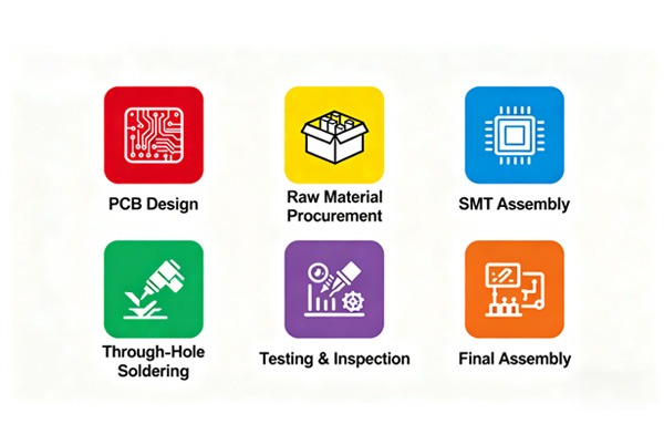
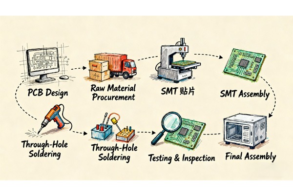
Solder Paste Stenciling (The Foundation)
The process begins with applying solder paste to the bare board using a stainless-steel stencil. Accuracy here is vital, as over 60% of PCBA defects originate from poor solder paste deposition. The paste must be perfectly aligned with the pads defined in your PCB design principles.
High-Speed Pick and Place (SMT)
Automated SMT machines pick SMD electronic components and place them onto the solder paste with micron-level precision. This stage is where high-density designs, such as HDI PCBs, achieve their compact form factor.
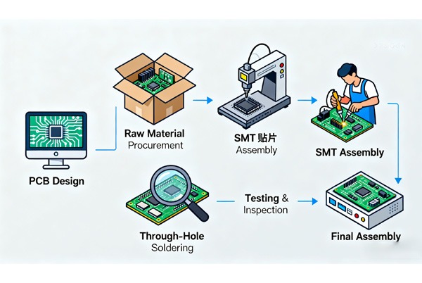
Reflow Soldering & Thermal Profiling
The board passes through a multi-zone reflow oven where the paste melts to form permanent electrical and mechanical joints. At Topfast, we customize the thermal profile based on the PCB stack-up design to prevent component overheating or “tombstoning.”
Inspection & Quality Control (AOI & X-Ray)
To ensure zero-defect manufacturing, every board undergoes:
- AOI (Automated Optical Inspection): Scans for missing components, polarity issues, or solder bridges.
- X-Ray Inspection: Essential for BGAs and QFNs where solder joints are hidden. This is a standard part of our high-end PCB assembly workflow.
Through-Hole Technology (THT) & Manual Assembly
For components requiring high mechanical strength (like connectors or large capacitors), THT is used via wave soldering or manual soldering. If you’re troubleshooting a prototype, you might need to test capacitors individually to verify circuit integrity.
5 Steps to Ensure a Smooth PCBA Processing Flow
- Conduct a Pre-Production DFM Review
Perform a Design for Manufacturing (DFM) check to ensure footprints match your SMD components.
- Optimize the Bill of Materials (BOM)
Verify that all components are available and have the correct manufacturer part numbers to avoid assembly delays.
- Define Solder Paste Requirements
Choose between leaded, lead-free (RoHS), or no-clean solder paste based on the end-use environment of the PCB design.
- Integrate Test Points
Add test points into your layout to facilitate In-Circuit Testing (ICT) and functional verification.
- Final Functional Testing
Once assembly is complete, perform a full functional test to ensure the PCBA meets all electrical specifications before shipping.
Frequently Asked Questions about PCBA Processing
A: A PCB is the bare circuit board without components, while a PCBA is the finished assembly with all components soldered and functional.
A: Standardizing component sizes (e.g., using 0603 instead of 0201) and minimizing unique parts in your BOM can significantly lower PCB assembly costs.
A: It is the only way to inspect solder joints under BGAs or inside HDI PCBs, ensuring there are no hidden shorts or voids.
A: Yes, this is called mixed assembly. SMT is typically performed first, followed by THT via wave soldering or manual soldering for through-hole parts.
A: Most failures are caused by poor PCB design optimization, incorrect solder paste volume, or inadequate thermal management during reflow.
Conclusion
Mastering the PCBA processing guide is key to launching successful electronic products. By focusing on DFM, precise SMT placement, and rigorous testing, Topfast ensures your designs are transformed into high-performance hardware.
Ready to start your production run? Get a Professional PCBA Quote from Topfast today.
Last Updated: March 2026 | Reviewed by: Topfast Engineering & Quality Dept.