A Comprehensive Analysis from Design and Manufacturing to Future Trends
In 2025, as artificial intelligence, electric vehicles, and sustainable technologies sweep the globe, the Printed Circuit Board (PCB) is no longer just a simple connector, but rather the core carrier that determines the performance, reliability, and cost of end products. This guide will go beyond listing basic concepts, taking you deep into the technological landscape of 2025. From material innovations and process evolution to selection strategies, it will fully equip you for hardware decision-making.
Table of Contents
PCB Laminate Structure Analysis
To understand a PCB, you must first visualise its internal layers, much like a CT scan. High-end designs in 2025 commonly adopt complex architectures like the following:
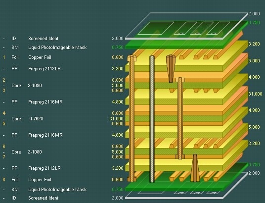
- Substrate (Dielectric Layer):
- The Evolution of FR-4: Standard FR-4 remains mainstream, but Halogen-Free FR-4 and High Tg (Glass Transition Temperature) FR-4 have become the default choices for high-reliability designs in 2025.
- The Rise of New Materials: To meet the demands of high-speed and high-frequency applications, the use of Polytetrafluoroethylene (PTFE) and Hydrocarbon Ceramic Filled Materials is growing rapidly, as they offer extremely low signal loss (Df).
- Copper Foil: Reverse Treat Foil (RTF) and Hyper Very Low Profile Foil (HVLP), due to their smoother surfaces, have become key technologies in 2025’s high-speed, high-frequency PCB designs for reducing signal loss (insertion loss).
- Solder Mask: Its role has expanded beyond “short-circuit prevention”. The trend in 2025 is towards using high-reflectivity white solder mask for LED boards and matte black solder mask to improve visual recognition during assembly.
Demystifying the PCB Manufacturing Process
The manufacturing process is the core determinant of PCB quality. Below is the 2025 industry-leading process flow and its critical control points:
- Design and Photo Plotting (Pre-production): Design for Manufacturability (DFM) Analysis is now commonly powered by AI in 2025, capable of automatically identifying over 90% of design flaws before production, significantly shortening R&D cycles.
- Inner Layer Imaging (Pattern Imaging and Etching): Laser Direct Imaging (LDI) technology, due to its exceptional precision and efficiency, has become the standard in 2025 for producing fine lines (line width/space < 3mil).
- Lamination: To handle the complexity of multi-stage HDI and rigid-flex boards, Vacuum Lamination and precise temperature/pressure profile control are essential to ensure no voids or delamination between layers.
- Drilling: High-Precision Mechanical Drilling and UV/CO2 Laser Drilling work in tandem to meet the needs of micro blind and buried vias, common in 2025’s High-Density Interconnect (HDI) designs.
- Plating: Pulse Plating technology provides more uniform copper deposition in the holes, significantly improving via reliability, making it the preferred process for high-reliability products (e.g., automotive electronics) in 2025.
- Surface Finish: Choices in 2025 are more refined, as detailed in the comparison below:
| Surface Finish | 2025 Application Scenarios | Advantages | Challenges to Consider |
|---|---|---|---|
| ENIG (Electroless Nickel Immersion Gold) | Universal choice, BGA, Connectors | Flat surface, Good solderability, Long shelf life | Requires strict control of the “Black Pad” phenomenon |
| ENEPIG (Electroless Nickel Electroless Palladium Immersion Gold) | Advanced Packaging, Wire Bonding | Compatible with soldering & wire bonding, prevents black pad | Relatively higher cost |
| ImSn (Immersion Tin) | High-Speed Digital Circuits | Excellent signal integrity, Moderate cost | Susceptible to scratching, Short storage life |
| ImAg (Immersion Silver) | High-Frequency Analogue Circuits, LEDs | Good signal performance, Low cost | Prone to sulfur tarnishing |
Three Major PCB Technology Frontiers for 2025
- Advanced HDI and mSAP Process: As IC pin pitches continue to shrink, the Modified Semi-Additive Process (mSAP) has become the core process for manufacturing cutting-edge PCBs with line width/space ≤ 40μm (approx. 1mil). This is the technological cornerstone of 2025’s flagship smartphones, AI accelerator cards, and high-end medical equipment.
- Embedded Component PCB: Embedding passive components like resistors and capacitors directly inside the PCB has moved from concept to small-scale production in 2025. It significantly increases wiring density, improves electrical performance, and enables product miniaturisation, making it a key focus for next-generation integrated design.
- Sustainability and Green PCBs: Facing increasingly stringent global environmental regulations, PCB factories in 2025 are actively implementing:
- Material Side: Use of halogen-free, phosphorus-free flame-retardant base materials.
- Process Side: Adoption of lead-free soldering and metal recycling technologies.
- Design Side: Promotion of Design for Disassembly to facilitate PCB recycling and reuse.
Select the optimal PCB solution for your project
- Performance Needs: What is your signal speed/frequency? (>10Gbps requires low-loss materials)
- Mechanical Requirements: Is device space extremely limited? Does it need to bend or flex dynamically? (Consider flexible or rigid-flex boards)
- Environment & Reliability: Will the product operate in high-temperature, high-humidity, or high-vibration environments? (Requires high Tg materials, stricter process standards)
- Budget & Supply Chain: What is the cost sensitivity while ensuring reliability? What is the strategy for coping with the fluctuating prices of raw materials like copper and epoxy resin in 2025?
Expert Action Advice: In 2025, early collaboration with manufacturers like TopFastPCB, which possess AI-DFM analysis capabilities and flexible production lines, is more critical than ever. We can provide engineering advice aligned with the latest 2025 IPC standards, helping you avoid risks at the source and ensuring your product gains a competitive edge in quality, cost, and delivery time.
Conclusion
The PCB is a blend of engineering and art. In 2025, it will be even more of a strategic discipline involving materials science, precision manufacturing, and supply chain intelligence. We hope this guide serves as a reliable map on your path to hardware innovation.
Frequently Asked Questions (FAQ) About PCBs
A: The green coating on a PCB is called the solder mask. It is not just a simple “paint”. Its core function is insulation, preventing solder bridges during the soldering process that could cause short circuits. It also protects the copper traces from oxidation and physical damage. While green is common, it can also be blue, red, black, and other colours.
A: Selecting the right PCB substrate is a critical decision, primarily dependent on your application:
General Electronics/Cost-Sensitive: Choose FR-4, the most economical and widely used option.
High-Frequency/High-Speed Circuits (e.g., RF, 5G): Require low-loss materials like Rogers or Taconic to minimise signal attenuation.
High-Power/High-Temperature Environments: Need High Tg (Glass Transition Temperature) FR-4 or metal-core substrates to ensure stability and heat dissipation under high temperatures.
Flexible or Bendable Applications: Should opt for flexible circuit board materials like Polyimide.
A: Surface finish is a crucial final step in PCB manufacturing, involving the coating of exposed copper pads with a protective layer. It is vital because it:
Prevents copper oxidation, ensuring the pads remain solderable during storage.
Provides a suitable surface for soldering, impacting the final assembly yield.
Affects signal integrity and long-term reliability. Common types include ENIG (Electroless Nickel Immersion Gold), Immersion Tin, and Immersion Silver, each with different cost and performance characteristics.
A: The main advantages of a 4-layer board over a 2-layer board are:
Better Signal Integrity: Allows for dedicated power and ground planes, providing stable voltage and low-noise reference planes, which reduces electromagnetic interference (EMI) between signals.
Higher Routing Density: The extra two layers provide more space for routing complex circuits, enabling a more compact design.
Improved EMC/EMI Performance: A solid ground plane can effectively shield signals, reducing electromagnetic emissions and susceptibility to external interference.
A: A via is a small hole in a PCB used to create an electrical connection between different circuit layers. The main types are:
Through-Hole Via: Passes through the entire PCB and can connect all layers.
Blind Via: Connects an outer layer to one or more inner layers but does not go through the entire board.
Buried Via: Located entirely within the inner layers of the PCB, connecting two or more internal layers, and is not visible from the surface.
Vias are essential for high-density, multi-layer PCB design.