What is an efficient PCB manufacturing process?
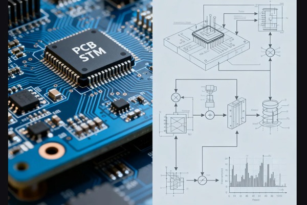
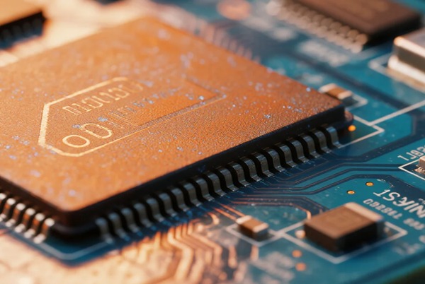
Printed circuit boards (PCBs) are core components of electronic devices, and the sophistication of their manufacturing processes directly determines product performance, reliability, and market competitiveness. The four key technologies of modern, efficient PCB manufacturing processes are panelization, modular production, automation and intelligence, and special process optimization. As an industry leader, Topfast provides professional PCB solutions in these areas.
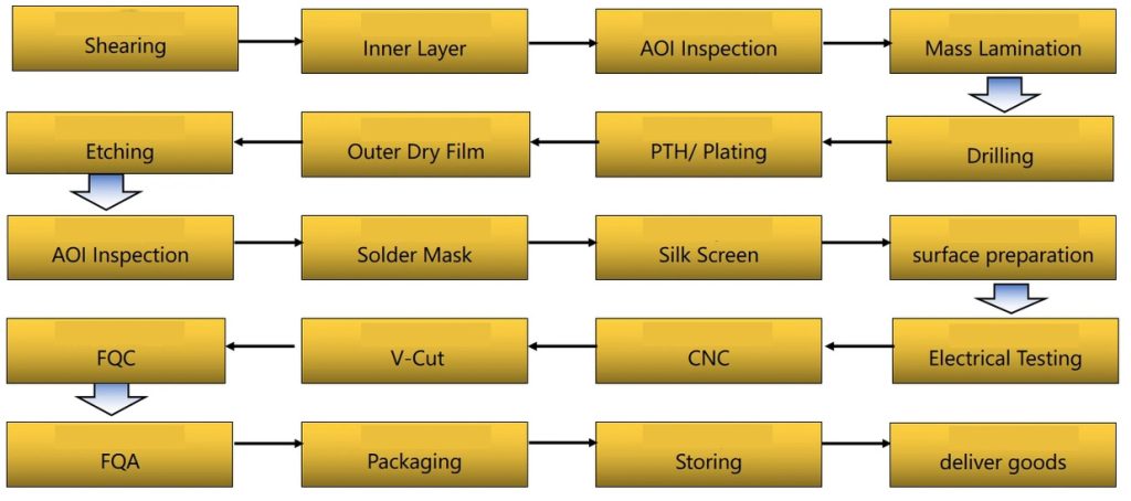
Table of Contents
Core Technologies of Efficient PCB Manufacturing
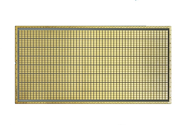
1. Panelization
Panelization technology is a core technology in modern PCB manufacturing that improves production efficiency and is key to doubling production efficiency. Topfast has achieved exponential growth in production efficiency by intelligently combining multiple PCB units into standard-sized panels. Our data show that using an optimized panelization solution can increase SMT placement machine efficiency by more than 300% while increasing substrate utilization to 85%, resulting in a significant reduction in material waste.
Topfast’s panelization process advantages
- V-CUT and Breakaway Tab Technology: Provides optimal connection solutions for different board types, ensuring separation accuracy.
- Smart Panelization Edge Design: Standard 5mm process edges with precise locating holes ensure stable operation of automated equipment.
- Mixed Panelization Technology: Allows different PCB models to be produced on the same panel, ideal for small-batch, high-variability market demands.
Our AOI inspection system ensures 100% quality control of panelized PCBs, guaranteeing every board meets stringent standards.
2. Modular Production
Topfast’s innovative modular production system breaks down the PCB manufacturing process into independent functional modules, enabling us to flexibly respond to diverse customer needs. This architecture allows us to quickly adjust parameters to accommodate various customization requirements.
- Parametric Plating System: Instant adjustments for different copper thickness requirements (1oz–6oz), reducing setup time by 87.5%.
- Smart Drilling Module: Laser drilling machines with 2,000+ parameter combinations reduce changeover time from 2 hours to just 15 minutes.
- Segmented Etching Line: Independent control of chemical concentration and temperature in each section ensures line width accuracy within ±10μm.
Our VCP (Vertical Continuous Plating) production line features a modular design, seamlessly switching between through-hole, blind via, and other process requirements to accommodate everything from standard multilayer boards to HDI boards.
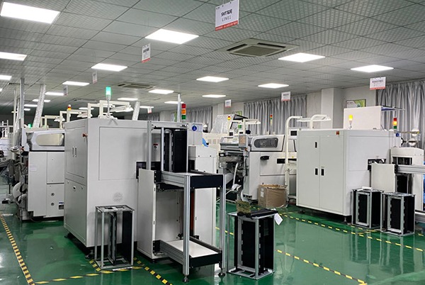
3. Automation & Intelligence
Topfast has its smart factory, which has achieved a leap in quality and efficiency through automated equipment and intelligent management systems, providing a double guarantee of quality and efficiency.
- Fully Automated Production Line: Automation from material cutting and drilling to surface treatment minimizes human intervention.
- MES Intelligent Scheduling System: Real-time production monitoring and dynamic resource optimization reduce typical lead times to just 3 days.
- 90%+ Equipment Utilization: Smart predictive maintenance maximizes uptime.
Our quality control system includes:
- Multi-Level Testing: Flying probe testing, AOI, X-ray, and functional testing.
- Real-Time Process Monitoring: Key parameters (e.g., etching rate, copper thickness) recorded every 30 seconds.
- Big Data Analytics: Optimizes process windows based on historical data to continuously improve yield.
4. Specialized Process Optimization
In response to increasingly complex technical requirements and high-end technical challenges, Topfast has developed a series of special process solutions.
- High-Density Interconnect (HDI) Technology:
- Laser blind via capability: Minimum hole size 50μm.
- Any-layer interconnects with trace/space down to 30μm/30μm.
- Supports 0.4mm-pitch BGA packaging.
- Special Material Processing:
- Dedicated production lines for high-frequency materials (Rogers, Taconic).
- Aluminum substrates with thermal conductivity up to 2.0W/m·K.
- Ceramic substrate processing thickness: 0.1–1.0mm.
- 3D Structured PCBs:
- Laser cutting precision: ±50μm.
- Rigid-flex multilayer stacking.
- Irregular-shaped panelization solutions.
Topfast’s vertical vacuum resin plugging machines and ceramic grinding lines provide hardware support for these specialized processes.
Topfast’s Professional Edge: 17 Years of Technical Expertise
As a PCB solutions expert with 17 years of experience, Topfast has built a comprehensive quality assurance system:
- End-to-End Process Control: 18 key quality checkpoints from design review to final testing.
- Advanced Inspection Equipment:
- High-precision flying probe testers (minimum test pitch: 0.1mm).
- X-ray inspection (BGA solder joint resolution: 5μm).
- AOI systems (defect detection rate: 99.9%).
- Certifications:
- ISO9001:2015 Quality Management System.
- UL Certification.
- IPC-A-600G Class 3 Standards.
Our rapid prototyping service delivers fully assembled samples in 72 hours, while small-batch production lead times are 40% shorter than industry averages.


Related Posts