What is AOI(Automated Optical Inspection)?
Table of Contents
What is AOI?
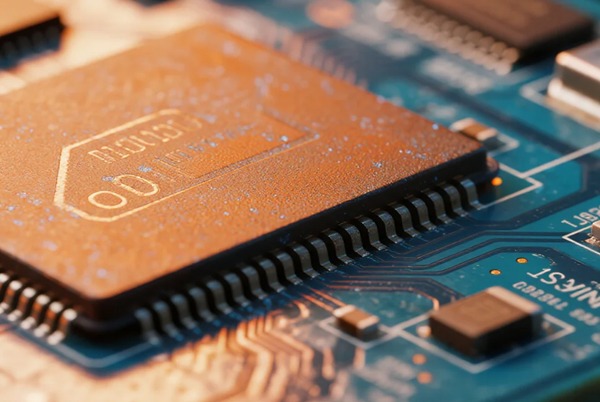
AOI (Automated Optical Inspection) is a high-precision industrial detection system based on machine vision, primarily used for quality control of printed circuit boards (PCBs). Its core principle involves combining high-speed optical imaging with intelligent algorithms to automatically identify PCB assembly defects (e.g., component misalignment, missing parts) and soldering issues (e.g., bridging, cold joints).
AOI System Working Principle
1. Image Acquisition Stage
- High-precision imaging: Utilizes industrial CMOS/CCD cameras with ring lighting to capture PCB surface features at micron-level resolution
- Multi-dimensional capture: Supports 2D inspection (solder joints/silkscreen) and 3D topography analysis (solder paste height/component coplanarity)
2. Image Preprocessing
- Noise suppression: Applies Gaussian filtering and morphological operations to eliminate optical interference
- Feature enhancement: Employs edge sharpening and HDR fusion to improve target area contrast
- Coordinate alignment: Performs CAD-to-image registration using fiducial marks as reference points
3. Intelligent Defect Detection
- Standards-based verification: Checks component placement/polarity/solder joint morphology against IPC-A-610 criteria
- Hybrid algorithms:
Traditional: Template matching, Blob analysis
AI-powered: CNN networks for detecting tombstoning, cold solder, etc.
4. Output & Feedback
- Tiered alerting: Triggers visual/audio alarms by defect severity (Critical/Major/Minor)
- System integration: Syncs NG results to MES with repair station coordinates
- Process optimization: Provides SPC data for reflow oven/pick-and-place machine tuning
AOI Technology Advantage
1. Limitations of Manual Inspection
Early PCB inspection relied on manual visual checks. However, with the rise of high-density interconnect (HDI) designs and mass production demands, manual methods face three critical challenges:
- Low reliability: Prone to fatigue and subjective judgment, with defect escape rates exceeding 15%
- Inefficiency: Inspection speed <0.5 boards/minute, incompatible with modern SMT line cycles
- Rising costs: Labor accounts for 8%-12% of total PCB costs, with lengthy training requirements
2. Core Detection Capabilities of AOI
Accurately identifies 7 major defect categories:
| Defect Type | Examples | Detection Accuracy |
|---|---|---|
| Component Placement | Missing, misalignment, and reversed polarity | ±25μm |
| Solder Joint Quality | Cold solder, bridging, and insufficient solder | 5% diameter tolerance |
| Lead Form Defects | Bent, lifted, non-coplanar leads | 15μm resolution |
Unique Advantages Over Traditional Methods:
- Eliminates test blind spots: Detects BGA underfill, 0201 components, and other areas inaccessible to ICT probes
- Closed-loop data analytics: Real-time defect classification (e.g., identifying 30% stencil printing defects) enables process optimization
3. Quantified Performance Advantages
| Metric | AOI Inspection | Manual Inspection | Improvement |
|---|---|---|---|
| Precision | Detects 0.01mm² defects | Human limit: 0.1mm² | 10x better |
| Speed | 20 boards/minute (dual-lane) | 0.3 boards/minute | 66x faster |
| Consistency | CpK ≥1.67 | CpK ≤1.0 | Yield ↑40% |
4. Smart Manufacturing Integration
- Real-time feedback: Triggers MES alerts with repair station coordinates (<2 sec response)
- Predictive maintenance: SPC-based trend analysis forecasts issues like stencil clogging
- Cost efficiency: Typical ROI <6 months with 50-70% scrap reduction
The critical role of AOI in SMT production lines
I. Four Key Inspection Nodes of AOI in SMT Process
- Post-Solder Paste Inspection (SPI-AOI Integration)
- Core function: Measures paste thickness (±5μm), coverage area, and bridging defects
- Preventive value: Early detection of stencil clogging/misalignment prevents reflow defects (60% defect interception rate improvement)
- Post-Chip Component Placement (After Chip Mounter)
- Focus: Missing, reversed, or misaligned 0201/0402 components (±15μm accuracy)
- Cost advantage: Rework cost at this stage is only 1/20 of the post-reflow correction
- Post-IC Component Placement (Fine-pitch Devices)
- Critical capability: Identifies QFP/BGA polarity errors and lead coplanarity (0.5° angular resolution)
- Process control: Real-time data exchange with pick-and-place machines for automatic offset compensation
- Post-Reflow Final Inspection (Comprehensive Defect Screening)
- Key challenges:
3D solder joint morphology detection (requires 10μm Z-axis resolution)
Inspection of shadowed areas (e.g., QFN bottom terminations) - Industry status: 92% detection rate vs. 99.5% for pre-reflow AOI
II. Technical-Economic Comparison: Pre-Reflow vs. Post-Reflow AOI
| Dimension | Pre-Reflow AOI | Post-Reflow AOI |
|---|---|---|
| Focus | Process prevention | Quality assurance |
| Key Metric | False call rate <0.1% | Escape rate ~8% |
| Cost Efficiency | $0.002/board | $0.15/board rework |
| Technical Challenge | High-speed dynamic inspection (≥45cm/s) | Complex 3D solder joint reconstruction |
III. Best Practice Recommendations
- Equipment Selection Strategy
- Pre-reflow: Prioritize high-speed AOI with on-the-fly technology (e.g., Koh Young KY8030)
- Post-reflow: Must incorporate 3D confocal microscopy (e.g., Omron VT-S730)
- Closed-Loop Data Application
- Establish SPC control charts (auto-trigger stencil cleaning when paste defects >3%)
- Feed placement offset data back to pick-and-place machines via MES (±7μm compensation accuracy)
- Future Evolution Trends
- Virtual AOI using deep learning (EDA-stage defect risk prediction)
- Multimodal inspection (X-ray + AOI data fusion for holistic solder joint modeling)
AOI Inspection Quick Reference Guide
1. Character Misjudgment
- Issue: False calls due to blurry/inconsistent component markings
- Solutions:
- Use multi-spectral imaging (visible + IR)
- Adjust grayscale tolerance (ΔE < 15)
- Reduce critical character checks
2. Inspection Blind Spots
- Common Blind Spots:
- Tall component shadows → 45° ring light + side lighting
- BGA bottom solder joints → Confocal microscopy layer scan
- Components <3mm from board edge → Design 5mm keep-out zone
3. Solder Joint Standards Debate
- Key Parameters:
- Chip components: Wetting angle 25°-55°, Xc/Xi=1.2-1.8
- QFP components: Solder fillet ≥50% lead thickness
- Design Rule:
  Pad extension = Component length × 0.25
  Minimum spacing = Avg. component height + 0.5mm
4. Implementation Results
- Typical improvements:
False call rate ↓70%
Inspection speed ↑25% - Emergency fix:
If excessive false calls → Disable character check or enable “Learning Mode”
5. Quick Troubleshooting Table
| Issue Type | Primary Fix | Backup Solution |
|---|---|---|
| Character errors | Adjust the grayscale threshold | Disable character check |
| Solder joint misses | Add side lighting | Manual recheck zone |
| Shadow interference | Rotate PCB 90° | Mark as an exclusion zone |
AOI Technology Applications and Industry Coverage
1. Core Application Fields
- SMT Electronics Manufacturing (Primary Domain)
- Inspection Targets:
Solder joint quality (voids/bridges/insufficient solder)
Component placement (misalignment/reversed/missing)
Polarity verification (tantalum capacitors/diodes orientation) - Industry Standards:
IPC-A-610 Class 3 (Aerospace/Medical grade)
Detection accuracy: ±15μm (0201 component level)
- Display Panel Production (LCD/OLED)
- Critical Inspections:
Pixel defects (bright/dark spots/line defects)
Alignment accuracy (Panel offset <3μm)
Adhesive uniformity (UV glue width tolerance ±50μm)
2. Broad Industrial Applications
| Sector | Typical Use Cases | Technical Features |
|---|---|---|
| Semiconductor Packaging | Wafer bump height inspection (±1μm) | 3D confocal microscopy |
| Automotive Electronics | Engine ECU solder joint 100% inspection (zero-defect requirement) | Vibration-proof inline system |
| Biomedical | Microfluidic chip channel integrity check | Sub-micron white-light interferometry |
3. Emerging Technology Integration
- Smart Factory Implementation
- MES system integration enables:
Real-time yield monitoring (data refresh rate ≤2s)
Adaptive detection thresholds (AI-driven parameter adjustment)
- Cross-Industry Expansion
- Food Packaging: Aluminum foil seal integrity check (0.1mm accuracy)
- Textile Industry: Fabric defect auto-sorting (30m/min speed)
4. Technology Selection Guide
- Electronics Manufacturing Priority:
- 3D SPI+AOI integrated systems (e.g., Koh Young KY8030)
- Minimum detectable component: 01005 (40μm×20μm)
- General Industrial Recommendations:
- Universal AOI systems should feature:
Multi-spectral lighting (for metal/plastic substrates)
IP54 protection rating (dust/oil resistance)
Conclusion
Automated Optical Inspection (AOI) technology, as a core quality control means in modern manufacturing, has expanded from traditional SMT electronics manufacturing to diverse fields such as LCD panels, semiconductor packaging, automotive electronics, and biomedical. Its core value lies in the combination of high-precision optical imaging (±15μm) and intelligent algorithms (e.g., deep learning) to realize the automated detection of solder joint defects, component placement errors and polarity issues, and at the same time, linkage with the MES system to form a closed-loop of data to promote the upgrading of intelligent manufacturing. In the future, AOI will be deeply integrated with X-ray and AI predictive maintenance to further break through the detection limit and become an indispensable “quality gatekeeper” in the era of Industry 4.0.


Related Posts