What is the difference between integrated circuits and PCB?
Table of Contents
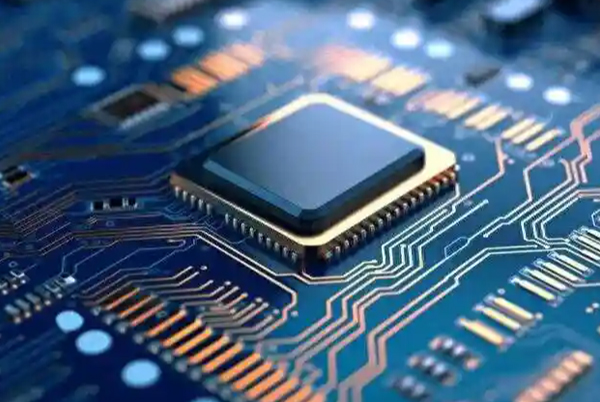
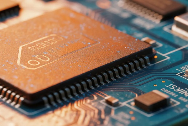
Integrated Circuits and PCBs
In today’s world, where electronic devices are ubiquitous, integrated circuits (ICs) and printed circuit boards (PCBs) form the physical foundation of all smart devices. However, these two technologies are often confused by non-professionals. What exactly are their fundamental differences? What roles do they play in electronic systems?
Fundamental Difference
Integrated Circuits (ICs) are the “brains” and “organs” of electronic systems:
- Integrate micro components such as transistors, resistors, and capacitors on semiconductor wafers
- Perform specific functions like signal processing, data computation, and storage
- Extremely small in size (nanometer to millimeter scale), requiring microscopes to observe internal structures
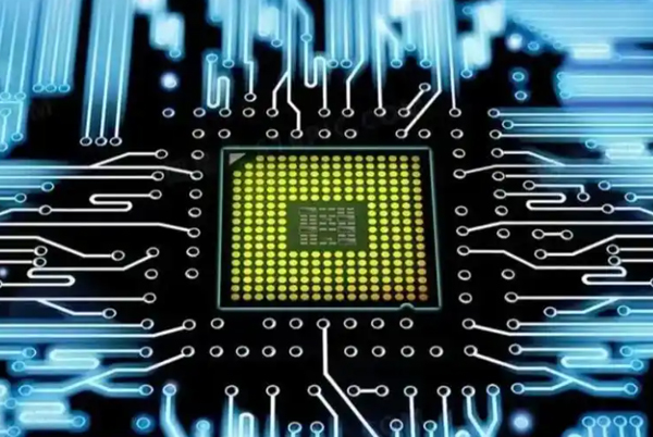
Printed Circuit Boards (PCBs) are the “skeleton” and “nervous system” of electronic systems:
- Provide a mechanical support platform for electronic components
- Establish electrical connections between components
- Macroscopic in structure (centimeter to meter scale), with visible circuit layouts
To use an analogy, if an electronic device were a human body, ICs would be the functional organs (brain, heart, etc.), while PCBs would be the skeletal system and neural network that connect these organs into a cohesive whole.
Structural Differences
The Microscopic World of ICs
- Material: Primarily silicon-based semiconductors
- Structure: Multilayered nanoscale circuitry
- Component Density: Modern ICs can integrate billions of transistors
- Typical Size: A few square millimeters to a few square centimeters
The Macroscopic Structure of PCBs
- Material: Fiberglass substrate with copper foil conductive layers
- Structure: Alternating layers of conductive traces and insulating material
- Component Density: Depends on soldering techniques and design standards
- Typical Size: From tiny wearable devices to large industrial control boards
Manufacturing Processes
Cutting-Edge IC Manufacturing
- Wafer Preparation: Growth of ultra-high-purity silicon crystals
- Photolithography: UV or extreme ultraviolet (EUV) lithography
- Doping Process: Ion implantation to alter semiconductor properties
- Metallization: Formation of nanoscale interconnects
- Packaging & Testing: Protecting the chip and connecting external pins
Mature PCB Production
- Substrate Preparation: Cutting copper-clad laminate material
- Pattern Transfer: Exposure and development of circuit designs
- Etching Process: Removal of excess copper foil
- Drilling & Plating: Creating interlayer connections
- Surface Finishing: Anti-oxidation and solder preparation
IC manufacturing requires Class 100/10 cleanroom environments, while PCB production has relatively lower environmental demands. This directly leads to significant differences in investment thresholds and industry distribution between the two.
Application Synergy Golden Combination
In real-world electronic products, ICs and PCBs work together seamlessly:
Smartphone Example:
- IC Components: Processor, memory, RF chips, etc.
- PCB Components: Motherboard, flexible circuits connecting modules
Industrial Control System:
- IC Components: MCU, ADC, power driver chips
- PCB Components: Multilayer control boards, power distribution boards
Notably, modern System-in-Package (SiP) technology is blurring the traditional boundaries between ICs and PCBs by integrating some PCB functions into chip packaging, driving electronic devices toward smaller sizes and higher performance.
Common misconceptions
- “ICs can replace PCBs”: False! ICs require PCBs for power and signal interconnects.
- “PCBs are the same as chips”: False! PCBs are merely carriers for chips.
- “ICs are more important than PCBs”: Misleading! Both play irreplaceable roles.
Future Technological Trends
IC Development Directions:
- Continued process miniaturization (3nm, 2nm)
- 3D stacking technology for higher integration
- Adoption of new semiconductor materials (GaN, SiC)
PCB Innovations:
- High-Density Interconnect (HDI) technology
- The proliferation of flexible/rigid-flex boards
- Advancement of embedded component technology
Key Differences Comparison
| Feature | Integrated Circuits (ICs) | Printed Circuit Boards (PCBs) |
|---|---|---|
| Function | Signal processing/data computation | Electrical connections/mechanical support |
| Structure | Nanoscale semiconductor structures | Micron-scale copper traces & insulation |
| Size | Millimeter-scale chips | Centimeter-to-meter-scale boards |
| Manufacturing | Class 100 cleanroom, photolithography | Standard factory, etching process |
| Cost | Extremely high R&D costs | Relatively lower costs |
| Repairability | Typically unrepairable | Components can be replaced |
Understanding the differences and connections between ICs and PCBs is fundamental to mastering modern electronics. Whether you’re involved in electronic product design, manufacturing, or simple repairs, this foundational knowledge will help you better grasp device principles and make more informed technical decisions.


Related Posts