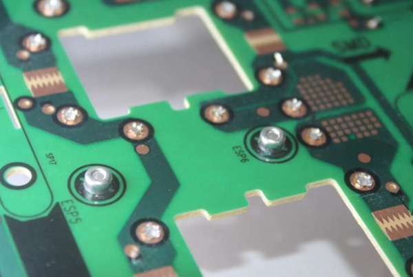
What is the purpose of unfilled solder pads on a PCB?
When manufacturing PCB circuit boards, electrical connections between electronic components and the circuit board are achieved by laying out wiring on the surface of the circuit board, installing electronic components, and then soldering them in place. Good connections and the strength of solder joints are critical to the normal operation of circuit boards.

Table of Contents
1. Design Purposes of Unfilled Solder Joints
- Test Point Functionality
- Electrical Testing: Exposed copper areas serve as test points for oscilloscopes, flying probe testers, and other similar devices.
- Process Verification: Post-reflow/wave soldering, test points validate process parameters.
- Special Design Requirements
- Heat Dissipation: Exposed copper in high-current traces improves thermal performance (requires current-carrying capacity calculations).
- RF Debugging: Unmasked impedance test points for high-frequency circuits (gold plating recommended).
2. Electrical Performance Impact Mechanisms
| Impact Dimension | Mechanism | Typical Scenario |
|---|---|---|
| Contact Resistance | Oxide layers increase impedance 3-5x | Excessive voltage drop in power circuits |
| High-Frequency Signal Loss | Impedance mismatches cause return loss (>3dB) | Increased bit error rates in 5G modules |
| Thermal Reliability | Higher thermal resistance raises junction temps by 10-15°C | Premature failure in power MOSFETs |
3. Solder Joint Quality Inspection Techniques
- Industrial-Grade Solutions
- 3D SPI: Solder paste thickness measurement (±5μm accuracy)
- Microfocus X-ray: Detects 0.2μm-level BGA voids (99.7% detection rate)
- Cost-Effective Solutions
- Red Dye Penetration: Low-cost crack detection (80% savings)
- Thermal Imaging: Identifies cold joints via temperature anomalies
4. Key Process Control Parameters
Reflow Soldering Profile (Lead-Free Process Example)
- Preheat: 150°C (1-2°C/s ramp rate)
- Soak Time: 90 sec (±5°C stabilization)
- Peak Temp: 245°C (30-45 sec duration)
- Cooling Rate: 3°C/s (prevents thermal shock)
Common Issues & Solutions
Q1: Signal integrity issues in high-frequency circuits—suspected unfilled solder joints?
A1: Use Time-Domain Reflectometry (TDR) to locate impedance discontinuities, then verify with X-ray. Recommendations:
- Use low-loss solder alloys (e.g., SnAgCu)
- Design test points with impedance compensation
Q2: How to quickly address cold solder joints in mass production?
A2: Implement a three-stage control method:
- Stencil optimization: Increase aperture size by 5%
- Nitrogen atmosphere: Maintain O₂ levels <1000ppm
- Inline AOI: Add side-view inspection
Q3: Exposed copper oxidation in humid environments, causing poor contact?
A3: Three-tier protection strategy:
- Primary: Electroless Nickel Immersion Gold (ENIG)
- Secondary: Local conformal coating (UV-curable resin)
- Tertiary: IP67-rated waterproof design


Related Posts