¿Cómo diseñar el control de impedancia para PCB?
Tabla de contenidos
La importancia del control de la impedancia de los circuitos impresos
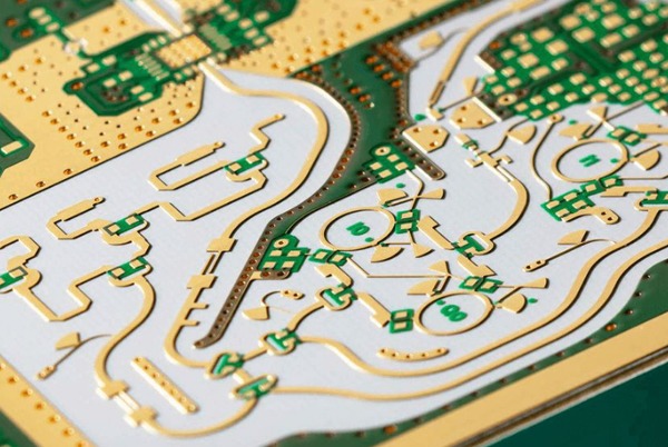
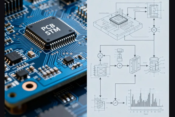
En los dispositivos electrónicos de alta velocidad actuales, la velocidad de transmisión de las señales es cada vez mayor, y el control de la impedancia de las placas de circuito impreso se ha convertido en un factor clave para determinar el éxito o el fracaso de un diseño. El desajuste de la impedancia puede causar problemas de reflexión de la señal, zumbido y rebasamiento, que afectan gravemente a la integridad de la señal. Según las estadísticas, más del 60% de los fallos en circuitos digitales de alta velocidad están relacionados con un control inadecuado de la impedancia. Por lo tanto, es esencial dominar la tecnología de control de impedancia de PCB.
Los cuatro pilares del control de la impedancia
1. Selección de materiales
“Elija el material adecuado, y estará a medio camino del éxito”-esto es especialmente cierto en el control de la impedancia:
- Materiales de alta frecuencia recomendados: Rogers RO4350B (εr=3,48), Isola I-Tera MT40 (εr=3,45) y otros materiales de bajas pérdidas son opciones ideales.
- Limitaciones del FR4 tradicional: Las grandes fluctuaciones de la constante dieléctrica (4,2-4,7) y la elevada tangente de pérdida (0,02) lo hacen inadecuado para aplicaciones por encima de 10GHz.
- Selección de láminas de cobre: La lámina de cobre de perfil bajo (lámina LP) reduce la rugosidad de la superficie en un 30% en comparación con la lámina estándar, lo que disminuye significativamente las pérdidas de alta frecuencia.
Consejo de experto: Para frecuencias de ondas milimétricas (24 GHz y superiores), considere materiales de pérdidas ultrabajas como Rogers RT/duroid 5880 (εr=2,2).
2.Diseño laminado
Un excelente diseño de apilamiento debe tener en cuenta:
- Estructura simétrica: Evita la deformación de la placa, como una disposición simétrica "señal-tierra-señal".
- Espesor entre capas: Valores típicos recomendados:
- Monoconector de capa superficial de 50Ω:Espesor dieléctrico de 5-6mil (ancho de traza de 8-10mil).
- Capa interior de un solo extremo de 50Ω:Espesor dieléctrico de 4-5mil (ancho de traza de 5-7mil).
- Planos de referencia: Asegúrese de que las capas de señal sean adyacentes a planos de tierra completos, evitando divisiones.
Estudio de casoUna placa de 6 capas optimizada para el apilamiento mejoró la integridad de la señal en un 40%:
Capa1:Señal (microstrip)
Capa2: Plano de tierra sólido
Capa3: Señal (stripline)
Capa4: Señal (stripline)
Capa5: Plano de masa
Capa6: Señal (microstrip)
Consulte a un profesional del diseño de PCB, un diseño científico de apilamiento de capas garantiza la fiabilidad de la placa de circuito impreso
3.Diseño del cableado
Fórmula de impedancia (aproximación microstrip):
Z₀ ≈ (87/√(εr+1,41)) × ln(5,98h/(0,8w+t))
Donde:
- Z₀: Impedancia característica (Ω)
- εr:Constante dieléctrica relativa
- h:Espesor dieléctrico (mil)
- w:Anchura del trazo (mil)
- t:Espesor del cobre (mil)
Consejos prácticos:
- Utilice las calculadoras de impedancia Polar Si9000 o Altium para realizar cálculos precisos.
- Siga la “regla de 3W” para pares diferenciales: Espaciado ≥ 3× ancho de traza.
- Coinciden con las longitudes de señal críticas dentro de una tolerancia de ±5 milímetros.
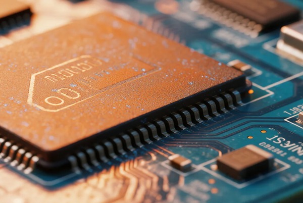
4.4. Proceso de fabricación
Al colaborar con Fabricantes de PCBConfírmalo:
- Tolerancia de impedancia: Típicamente ±10%, ±7% para aplicaciones de gama alta.
- Espesor del cobre acabado: 1oz de cobre ≈ 1,4mil (35μm) de espesor real.
- Variación del espesor dieléctrico: Normalmente dentro de ±10%.
- Acabado superficialENIG es mejor que HASL para aplicaciones de alta frecuencia.
Problemas comunes de control de la impedancia y soluciones
Problema 1: Discontinuidad de la impedancia inducida por la vía
Soluciones:
- Utilice el taladro de retroceso para eliminar el sobrante de la vía.
- Añada vías de tierra cerca de las vías de señales críticas (espaciado <150mil).
- Emplear microvías (<6mil) para reducir los efectos parasitarios.
Problema 2: Desajuste de la impedancia de la zona de transición del conector
Soluciones:
- Diseñe trazados cónicos para transiciones de impedancia suaves.
- Utilice estructuras de guía de ondas coplanares para mejorar la continuidad de tierra.
- Seleccione conectores de impedancia adaptada (por ejemplo, la serie SEARAY de Samtec).
Problema 3: Radiación en los bordes de la placa que provoca fluctuaciones de impedancia
Soluciones:
- Aplique la “regla 20H”: Plano de potencia insertado por 20× de grosor dieléctrico.
- Añadir suelo a través de matrices a lo largo de los bordes (espaciamiento <λ/10).
- Aplicar estructuras de banda prohibida electromagnética (EBG) para suprimir la radiación de borde.
Caso práctico: Optimización de la impedancia del canal SerDes a 10 Gbps
Desafío: Una PCB de conmutación de empresa presentaba errores de datos intermitentes.
Análisis:
- Las pruebas TDR revelaron una variación de impedancia del 15%.
- Causa principal: Insuficientes vías de tierra alrededor de los pares diferenciales.
- Las trazas superficiales no tenían en cuenta los efectos de la máscara de soldadura.
Solución:
- Aumento de la densidad vía terrestre (una por cada 200mil).
- Ancho de traza ajustado para compensación de máscara de soldadura (5mil→4,8mil).
- Conmutado a máscara de soldadura de baja Dk (εr=3,0).
Resultado: La variación de la impedancia se reduce al 5% y la tasa de error binario aumenta 100 veces.
Diseño profesional de control de impedancia consultoría para salvaguardar su diseño electrónico.

Tecnologías emergentes
- Materiales de muy baja pérdidapor ejemplo, Panasonic MEGTRON6 (Df=0,002).
- Tecnología dieléctrica híbrida: Combinación de materiales con diferentes valores Dk para la optimización de la impedancia localizada.
- Placas de circuito impreso en 3D: Habilitación de estructuras de impedancia graduada.
- Diseño asistido por IAAutomatización de la optimización de redes de adaptación de impedancias.
Lista de comprobación del ingeniero
Antes de someterlo a la fabricación de placas de circuito impreso, verifíquelo:
Confirmación con el fabricante de las especificaciones del material y las capacidades del proceso.
Simulación de impedancia de redes críticas.
Cumplió los requisitos de coincidencia de longitud de par diferencial.
Optimizado mediante estructuras.
Cupones de prueba diseñados.
Especificaciones de impedancia documentadas.
Con el rápido desarrollo de las tecnologías 5G, AI e IoT, la demanda de integridad de la señal de alta velocidad seguirá creciendo. Si domina la tecnología básica de control de impedancia de PCB, podrá destacar en el diseño de PCB de alta velocidad y garantizar la estabilidad y fiabilidad de sus productos.


Entradas relacionadas